Hydrogen Fracturing Process
- Cage Wiring Harness Analysis (20YA/J)
- PC9XA - Variable Voltage Pulse Circuit
- PC9XB - Variable Frequency Generator Circuit
- PC9XC - Variable Gate Circuit
- PC9XD - Voltage Regulator Circuit
- PC9XE - Sequential Gate Card
- Hydrogen Fracturing Process Book Link
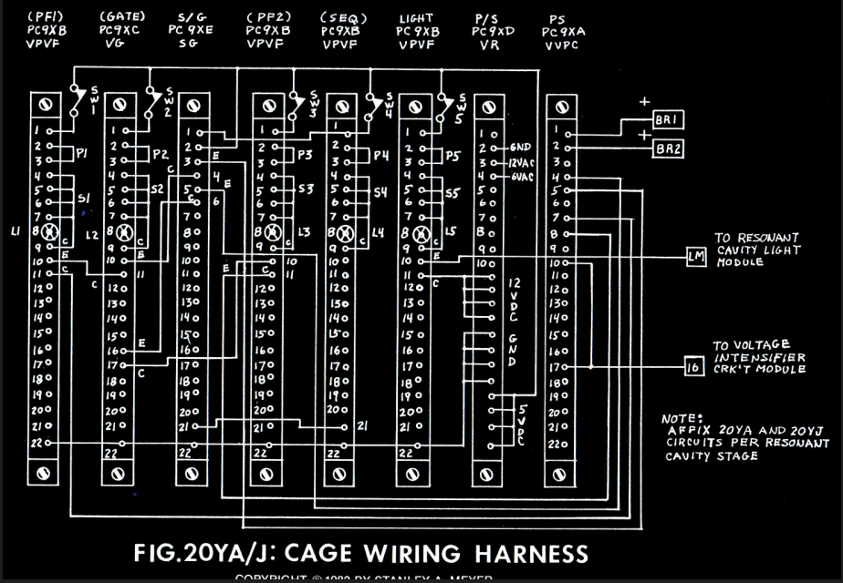
Cage Wiring Harness Analysis (20YA/J)
As of 5/7/23 boards are being put into production for analysis. Current analysis is subjected to change with future experimental results.
PC9XA - Variable Voltage Pulse Circuit
PC9XA - Variable Voltage Pulse Circuit
Circuit Analysis
Schematic:

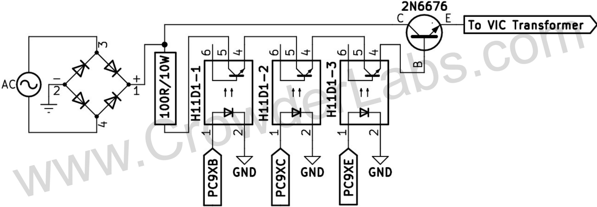
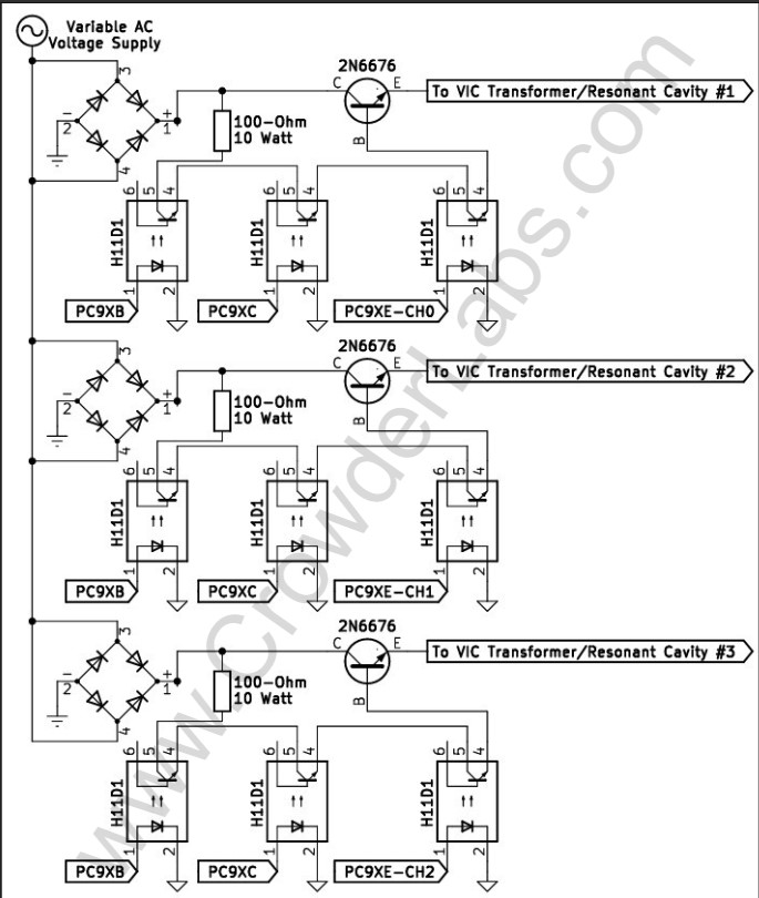
The circuit is composed of three independent power NPN-BJTs circuits. The 2N6676 was specified by Stan, however, any of appropriate rating or even modern N-Channel MOSFETs can be used. A rectifier stage produces a variable positive unipolar-pulsating waveform. Each circuit stage has a minimum of two optocouplers that provide electrical isolation between driver and waveform generation means. One provides a frequency pulse train (“Pulse Train”), the second one provides a gating frequency (“Gate”) that controls how many frequency pulses are applied to the base of the driver component. A 100Ω/10W resistor provides a small resistance, as the required base current for the driver BJT is larger than a Darlington pair for example.
Majority of the current limiting is provided by optocoupler waveforms. Using N-Channel MOSFETs would provide additional isolation given the nature of their capacitance coupling. Greater signal clarity would also be afforded by using MOSFETs. Two interesting observations present themselves in regards to the above schematic. One, a smoothing capacitance is not explicitly shown. However, in order to produce specific waveforms for VIC operation, this would be a necessity. Second, the power BJT is an NPN type, which typically are used in low-side switching applications. The schematic illustrates a high-side switching mode.
PC9XA - Variable Voltage Pulse Circuit
Stan's Original Literature
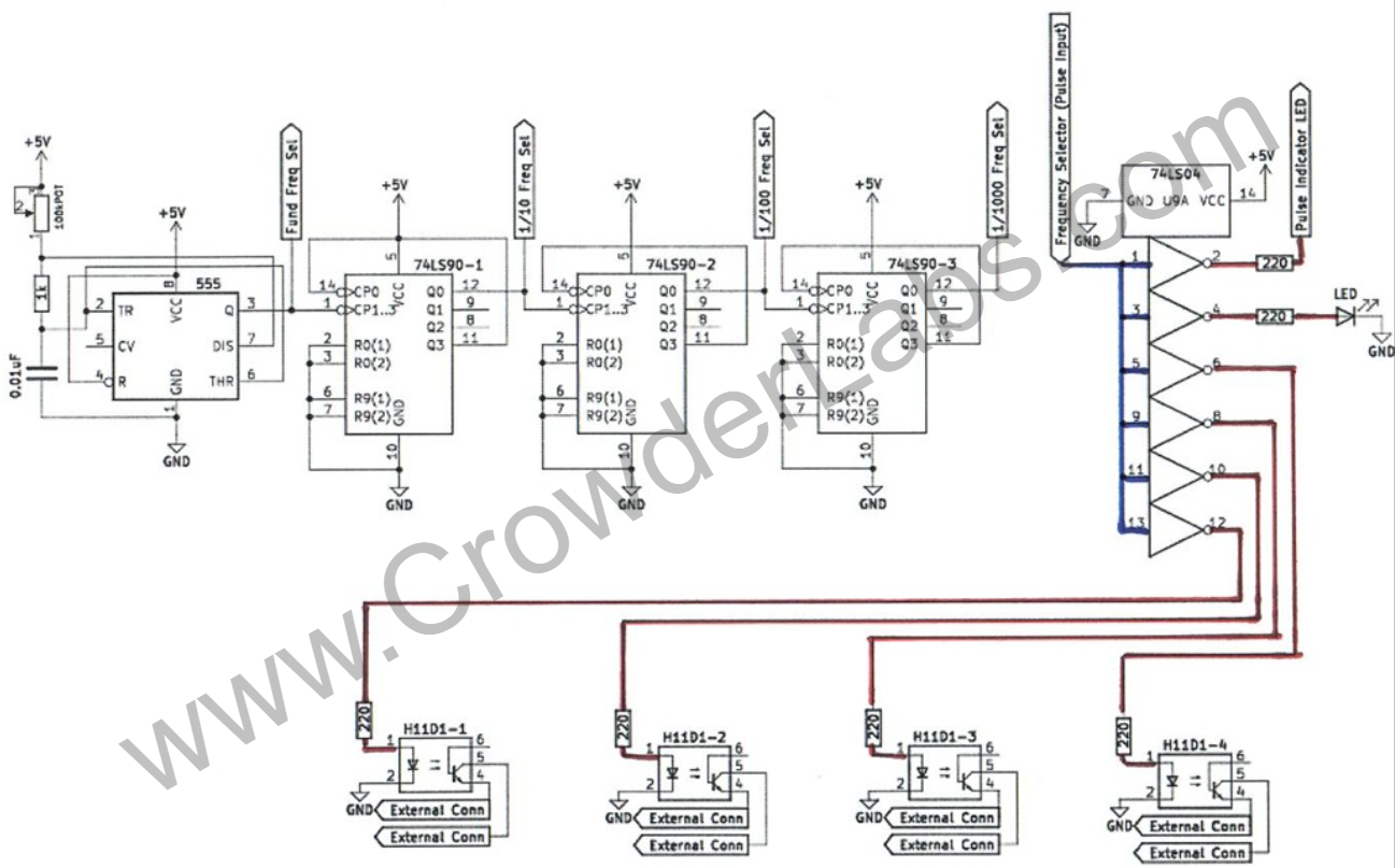
PC9XB - Variable Frequency Generator Circuit
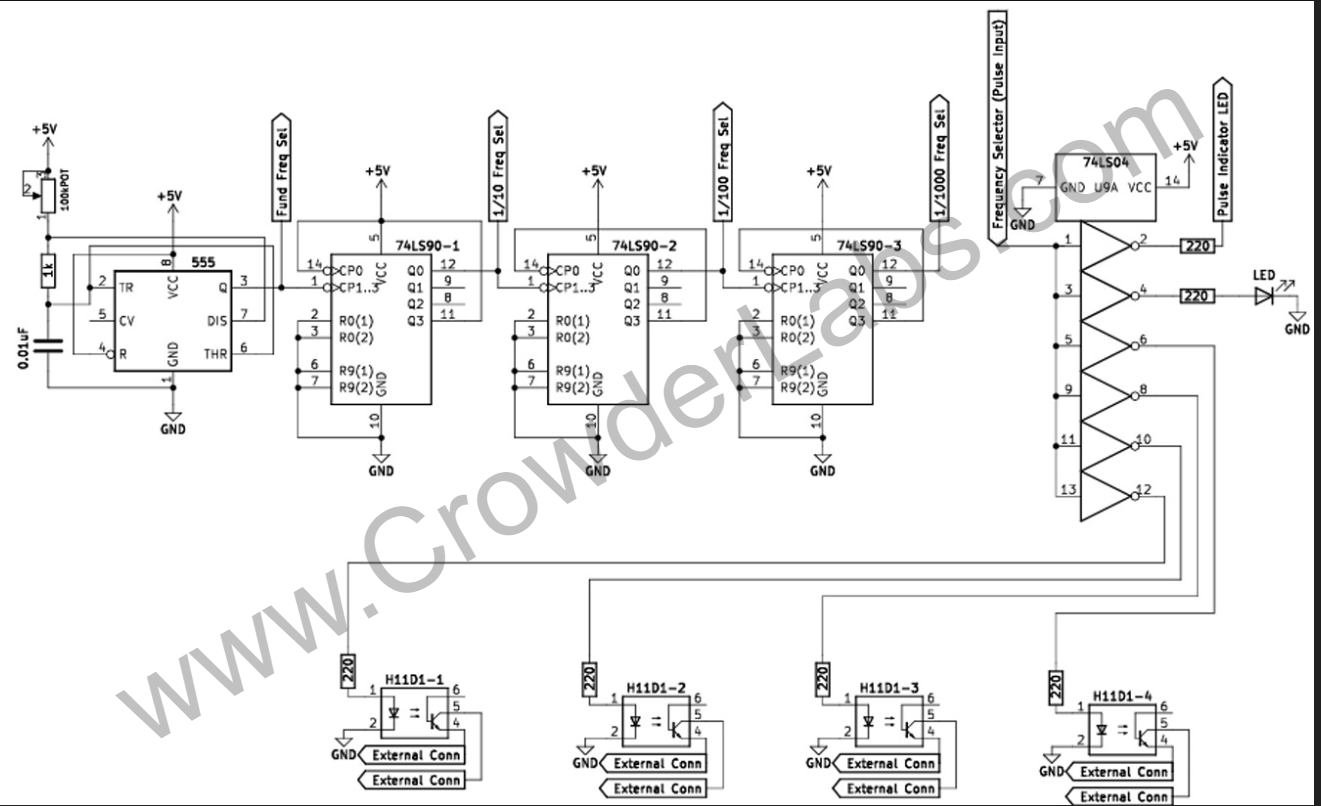
PC9XB - Variable Frequency Generator Circuit
My Circuit Analysis
Schematic:
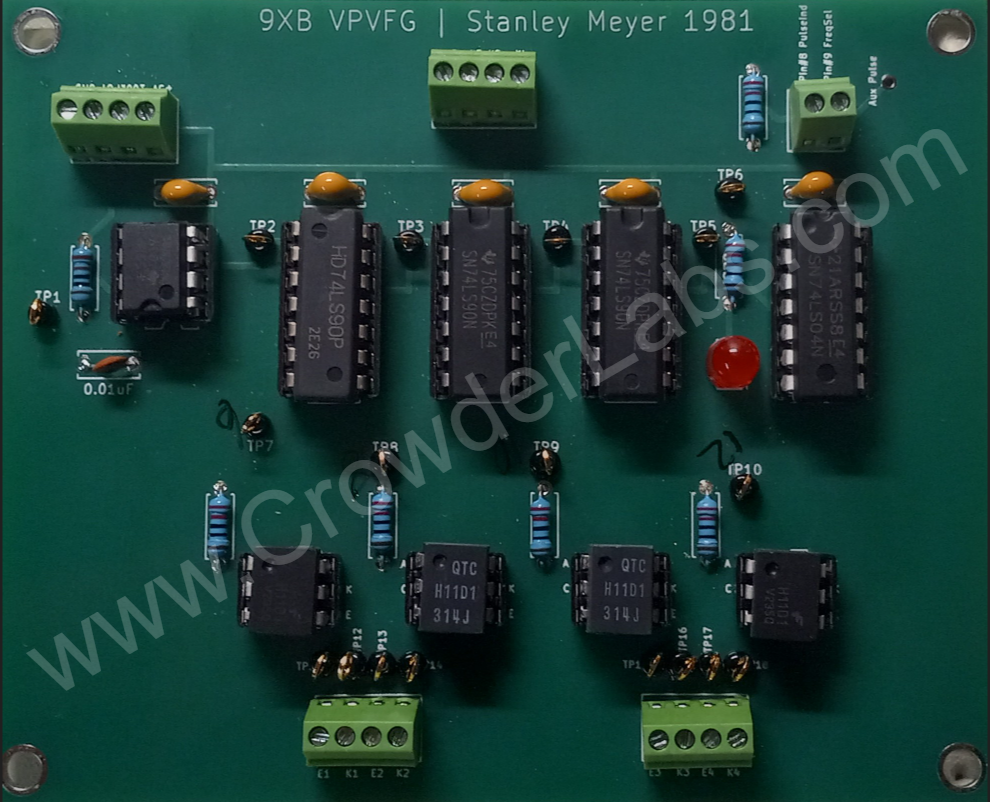
Replica PCB Top:
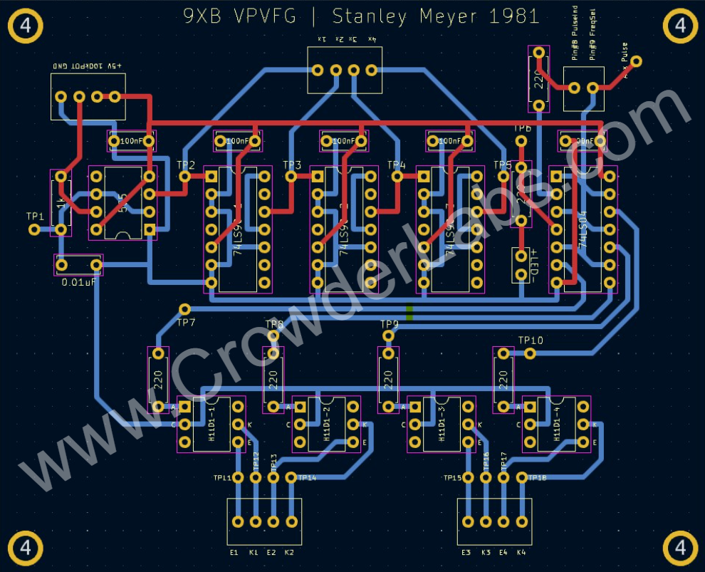
Replica PCB Traces:
555 Operation:
The pulsing of the circuit is produced by the 555 in astable operation mode, shown in Figure 1 below. Frequency is determined by the RC time constant, produced from the values of the potentiometer (0Ω-100kΩ), R1(1kΩ) and C1(0.01uF = 10nF). As the potentiometer has its resistance varied from minimum (0Ω) to maximum (100kΩ) the time it takes to charge up C1 is varied proportionately.

Decade Counter (7490/74LS90) Operation:
The 7490, or 74LS90 contains a divide by 2 and divide by 5 stages. These two stages are connected to form a divide by 10. Internally, networks of rising edge triggered flip flops are shifting. Figure 2 below illustrates each 7490 connections to achieve divide-by-ten operations.

Oscilloscope Waveforms:
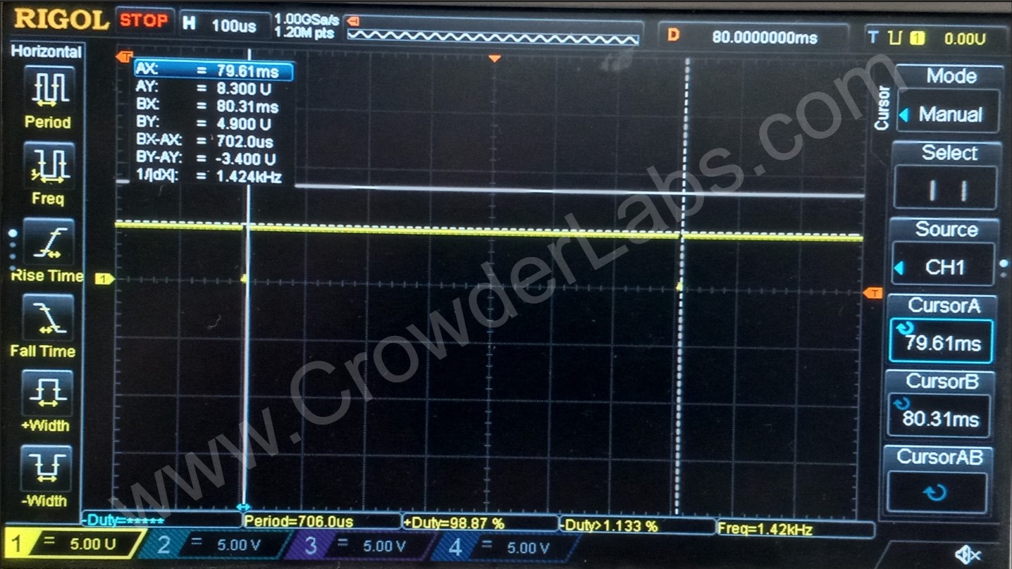
Pulse generation, supplied by the 555, produces a variable frequency output (pin #3). Given the circuit component values, varying the frequency also leads to a variance in duty cycle. Figure 3 below shows the measured duty cycle of ~1kHz. Scope measures 98.87% HIGH and 1.13% LOW.
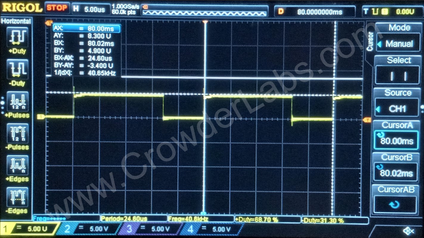
Below shows the duty cycle measurement of the fundamental frequency adjusted to ~40kHz. Scope measures 68.70% HIGH and 31.30% LOW.
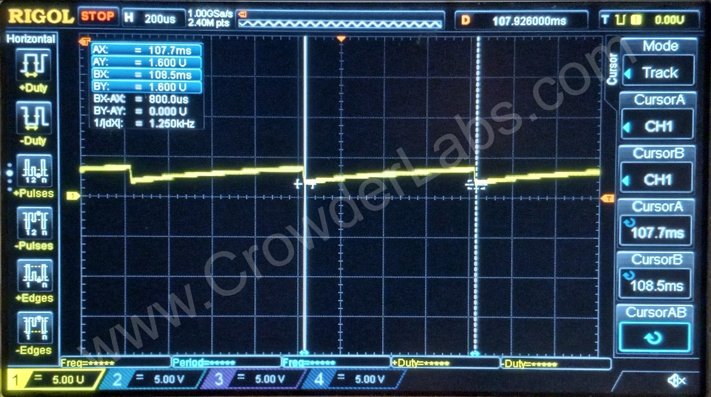
Frequency of the pulse is related to the period of the RC curve. Components of the RC curve (potentiometer and capacitor (0.01uF) determine this period. Figure 5 below demonstrates the longer period (800uS) for a lower frequency. In this capture, the frequency is 1.25kHz. To derive frequency from the period, the formula F = 1/T is utilized. Where ‘T’ is representative of the period time value. Therefore: F = 1 / 0.000800S, F = 1,250Hz.
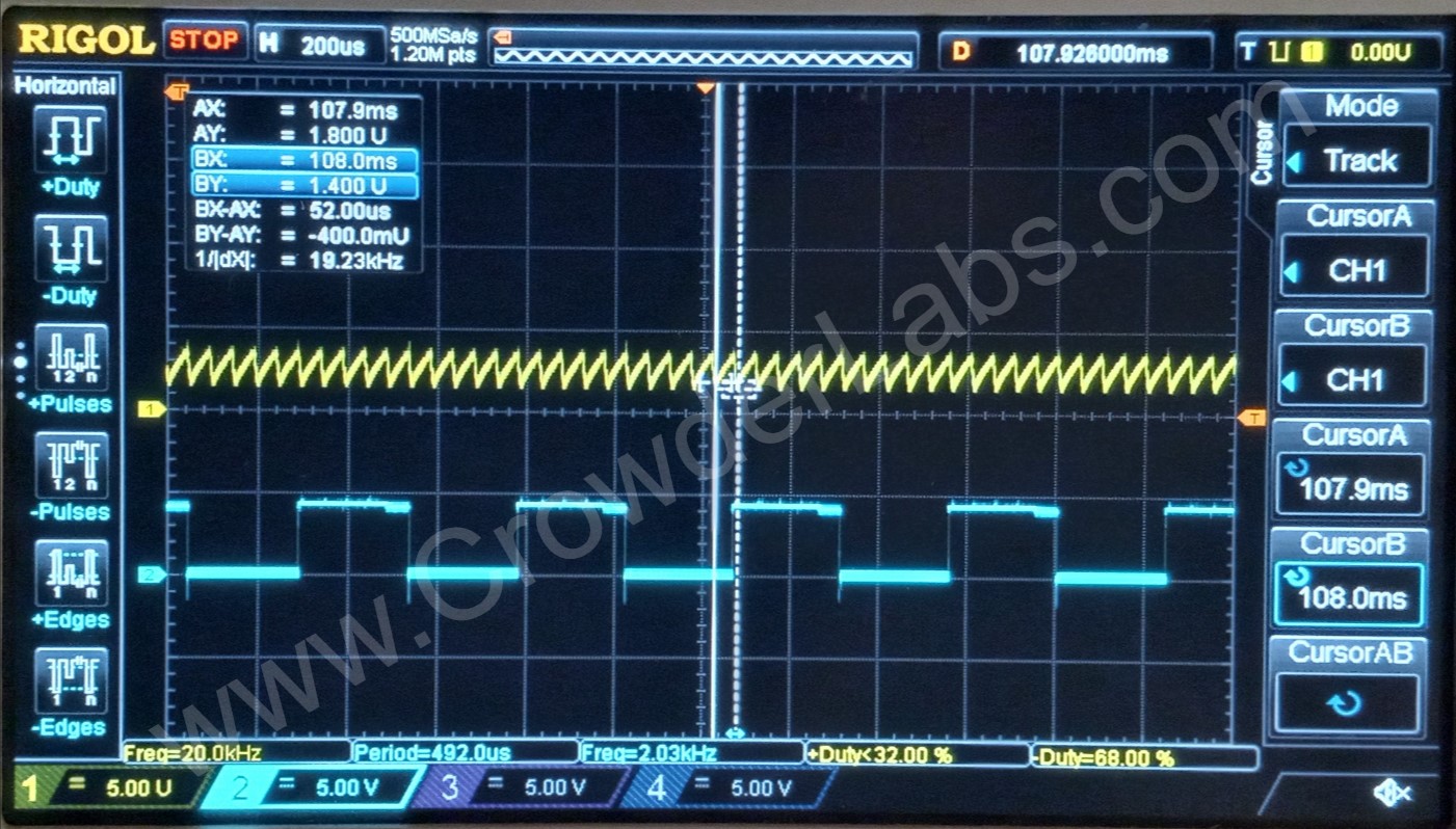
The picture below demonstrates the RC curve for a higher frequency. In this capture, the frequency is ~20kHz. Higher frequencies have lower period time values. Notice that both scope shots are on the same time base, 200uS per division. This was intentionally done to show how the RC curve is occurring much faster compared to the 1.25kHz scope shot above. Comparing the two further demonstrates the linear relationship between RC charging time and frequency.
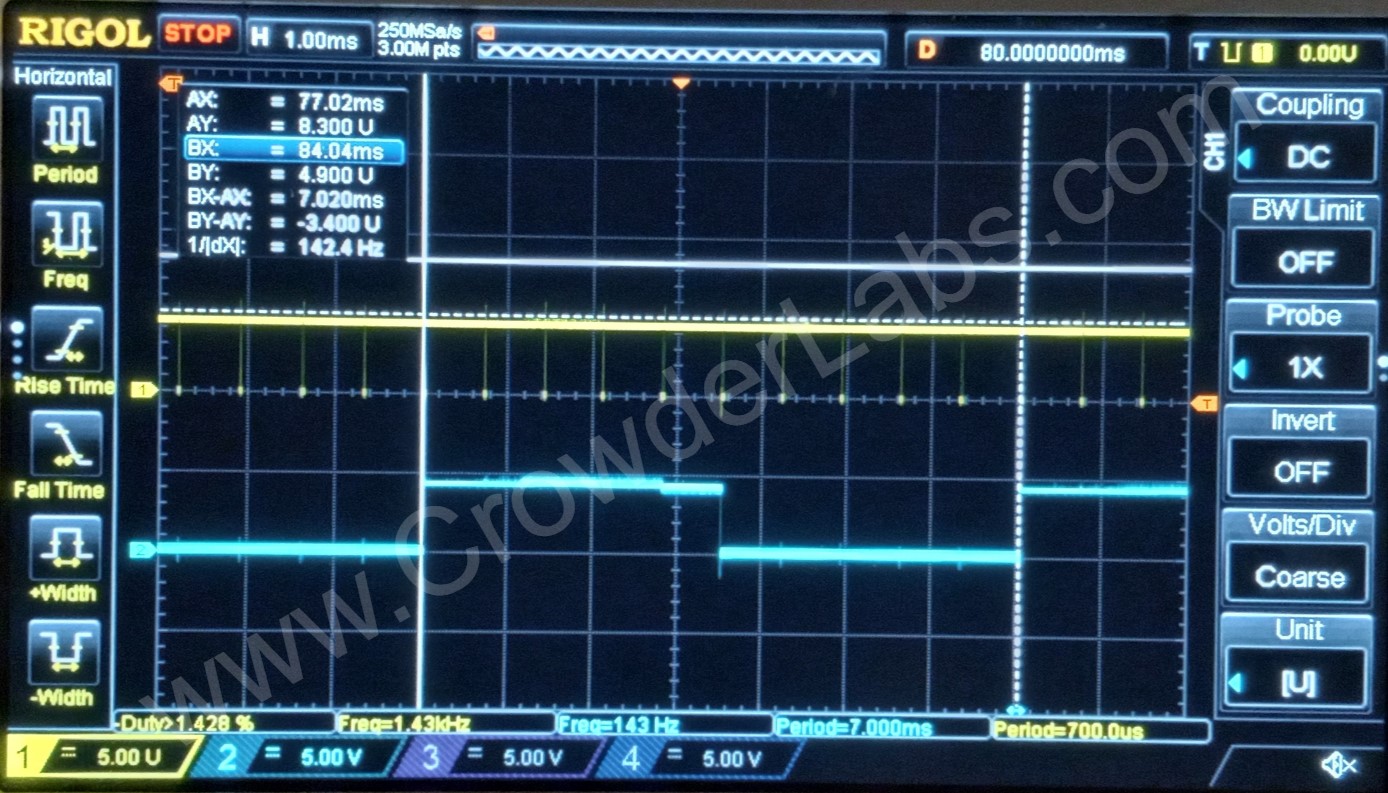
The 555 output (pin #3) frequency enters into the input (pin #1) of the first binary counter (74LS90-1), which is in a divide-by-ten arrangement. The counter begins the process of dividing the fundamental frequency by ten and conditioning the duty cycle to a fixed 50%. The output (pin #12), provides a frequency that is ten times less (1/10) that of the fundamental, and an external tap for selection of this frequency. The picture below captures this first division. Channel one (yellow trace) shows the fundamental frequency as discussed earlier. Channel two (blue trace) shows the divided-by-ten frequency. Channel one has a measured frequency of 1.43kHz and a period of 700uS. Channel two has a measured frequency of 143Hz and period of 7mS. Finding the quotient between these two, the measurements are ten divisions between one another: 1,430Hz / 143Hz = 10; 7mS / 700uS = 10. This frequency output (143Hz) is connected with the input (pin #1) of the second divide-by-ten counter (74LS90-2).
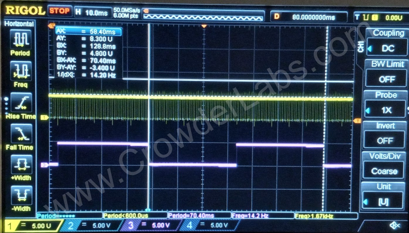
This second counter begins the process of dividing the fundamental frequency by one hundred. The output pin (#12), provides a frequency that is one hundred times (1/100) less than that of the fundamental. Another external tap is provided for selection of this frequency. As shown in Figure 8 below, channel one (yellow) represents the fundamental. Channel three (magenta) represents the division of one-one hundredth. The fundamental frequency is measured at 1.42kHz. The one-one hundredth division is measured at 14.20Hz.
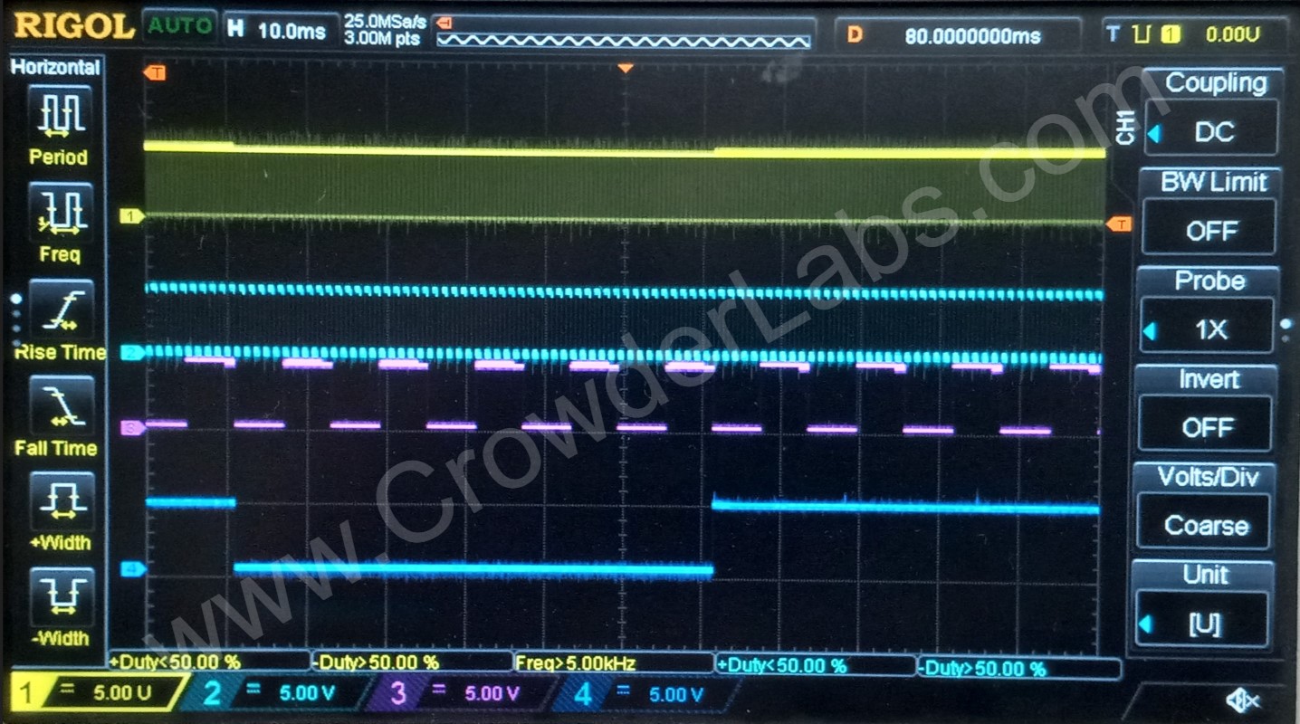
Below is a scope shot showing a comparison between all four channels.
A rotary switch provides the input, of whichever frequency is desired, into the inputs (pins #1, #3, #5, #9, #11, #13) of the hex inverter (74LS04). All of the inputs are connected together to synchronize the associated outputs. These outputs are logically inverted from the input pulse polarity as shown below. The input channel is represented by yellow trace. Other traces represent outputs to three of the four optocouplers.
First output (pin #2) is connected to a series 200Ω, ¼ watt resistor which provides current limiting (20mA) to the cathode of an externally mounted LED. This external LED provides visual indication of the frequency received by the optocouplers. Second output (pin #4) is connected to a series 200Ω, ¼ watt resistor which provides current limiting (20mA) to the cathode of the PCB mounted LED. This LED provides visual indication of the frequency received by the optocouplers. Four other outputs (pins #6, #8, #10, #12) are connected to a series 200Ω, ¼ watt resistor which provides current limiting (20mA) to the anode of their respective optocouplers (H11D1-1, H11D1-2, H11D1-3, H11D1-4).
When the 74LS04 output logical states are HIGH (1), the associated optocoupler’s internal LED turns on, which influences the base of the transistor, producing conduction on the output side. Conversely, when the 74LS04 output logical state are LOW (0), the associated optocoupler internal LED turns off, having been reversed biased. The optocouplers perform electrical isolation between the pulsing circuitry and their respective output terminals. The four optocouplers are used to provide pulsing for other circuitry that will be expanded upon in other sections. The schematic details which pin number is associated with the collector and emitter of the associated optocoupler.
Logical Flow - Phase 1:
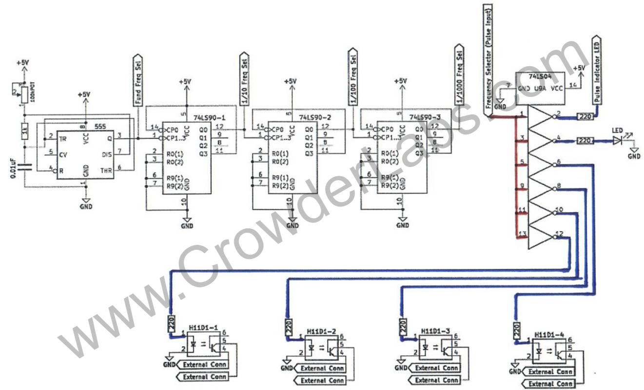
Logical Flow - Phase 2:
PC9XB - Variable Frequency Generator Circuit
Stan's Original Literature
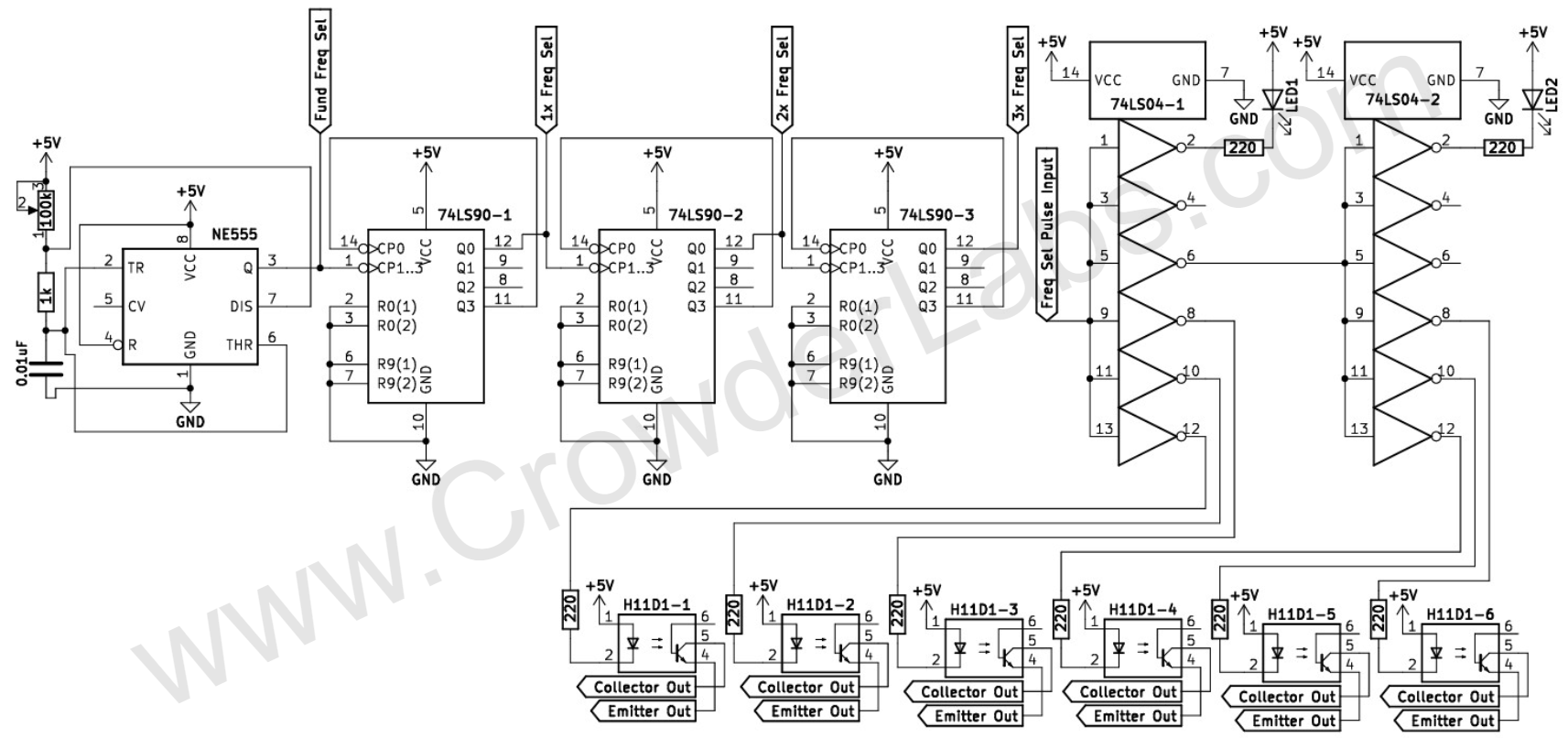
PC9XC - Variable Gate Circuit
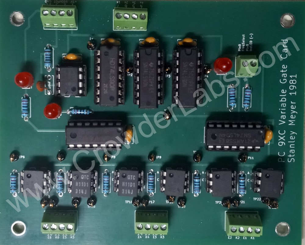
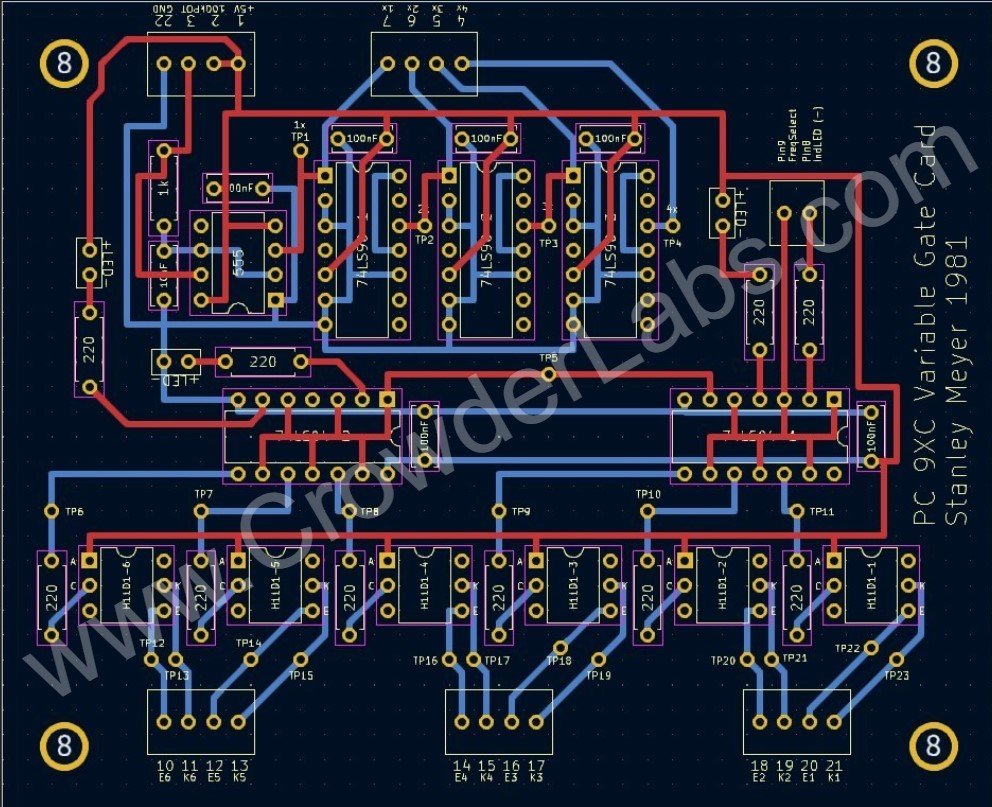
PC9XC - Variable Gate Circuit
My Circuit Analysis
YouTube video: PC9XC Variable Gate Circuit
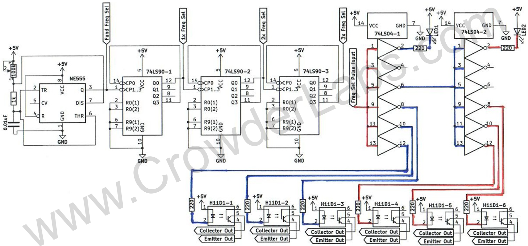
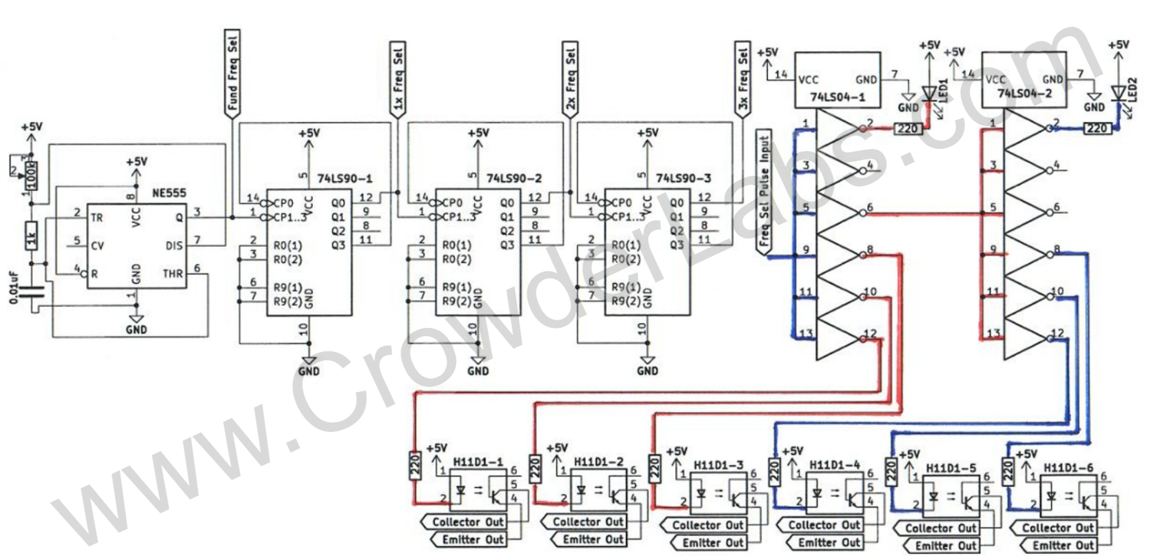
Schematic:
Replica PCB Top:
Please note that decoupling capacitors were added across each IC for stability and noise reduction. LEDs visually indicate when the hex inverters (74LS04-1/74LS04-2) are in opposing polarity. Photos demonstrating this functionality are within this section. PCB trace layers are shown in the photo below.
Replica PCB Traces:
Explanation:
The circuit includes an integrated variable frequency generator, with a 50% duty cycle provided by three divide-by-ten counters (74LS90), the same circuit as the PC9XB. The pulse train is communicated to two hex inverter (74LS04-1 & 74LS04-2) stages that produce 180-degree phase shifted output pulses. Put more simply, this circuit performs a flip-flopping function. Optocouplers provide isolation between control circuitry and the switching applications that will be covered herein. Having two optocouplers in series, controlling PC9XA driver BJT, produces a two input “AND” gate.
The aforementioned description of duty cycle adjustment is slightly misleading. As the frequency is decreased, the number of pulses, delivered by the PC9XB, to the excitor array is increased. Conversely, as the frequency is increased, the number of pulses is decreased. In both cases, the off time is equal to the on time due to the fixed 50% duty cycle. A better understanding can be ascertained by viewing Stan’s reference to “duty-cycle” variability within the scope of controlling the quantity of frequency pulses applied to the electrode pair.
Stan's Applications:
1.) Voltage Intensifier Circuit 9XA: Adjusting the number of pulses applied to the power transistor driving the VIC coil. Can facilitate several different pulse applications including continuous, gated and sequenced.
2.) Dual Voltage Pulsing Circuit: Adjusting the number of pulses applied to their associated power transistors driving the VIC coil. Providing two independently varied voltage pulse waveforms.
3.) Electron Extraction: Providing alternating switching between applying step charging waveform to gas resonant cavity positive electrode and applying positive potential to resistive element to cause liberated electron consumption.
4.) Steam Resonator Circuit: Provide switching to associated power transistor to produce alternating application of positive polarity to electrodes.
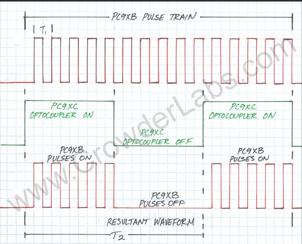
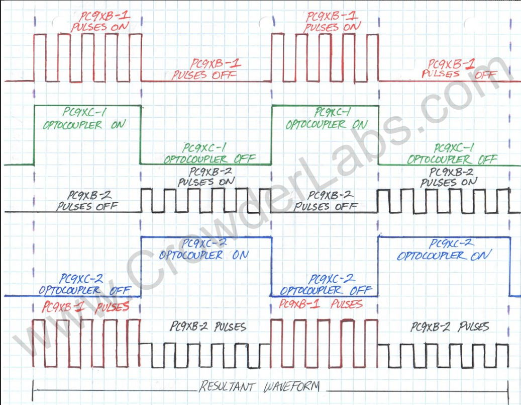
Referencing the schematic below, optocoupler “H11D1-2” controls the number of pulses per unit of time from the frequency generator, PC9XB, to be applied to power transistor’s base. Diagram 1 illustrates the waveform produced. While five pulses per half cycle are shown, both circuit’s frequencies are independently adjusted, resulting in a lack of synchronization without precise adjustments. The period of the PC9XB optocoupler pulse train is represented by T1, while T2 represents the period of the PC9XC optocoupler pulse train. It can be seen that both are fifty percent. Voltage of the resultant waveform is independently adjustable via variable transformer.
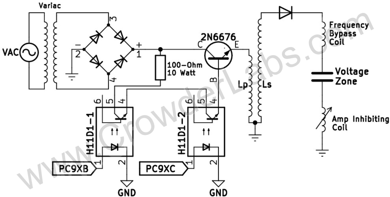
Diagram 1:
The picture below, shows another embodiment. Four separate circuits, two PC9XB’s and two PC9XC’s are utilized to produce two independently adjustable voltage gated pulse trains that are applied to a resonant cavity of a spherical geometry. Diagram 3 illustrates the waveforms during circuit operation.
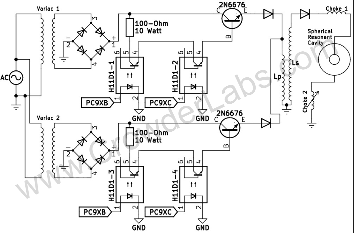
Diagram 2:
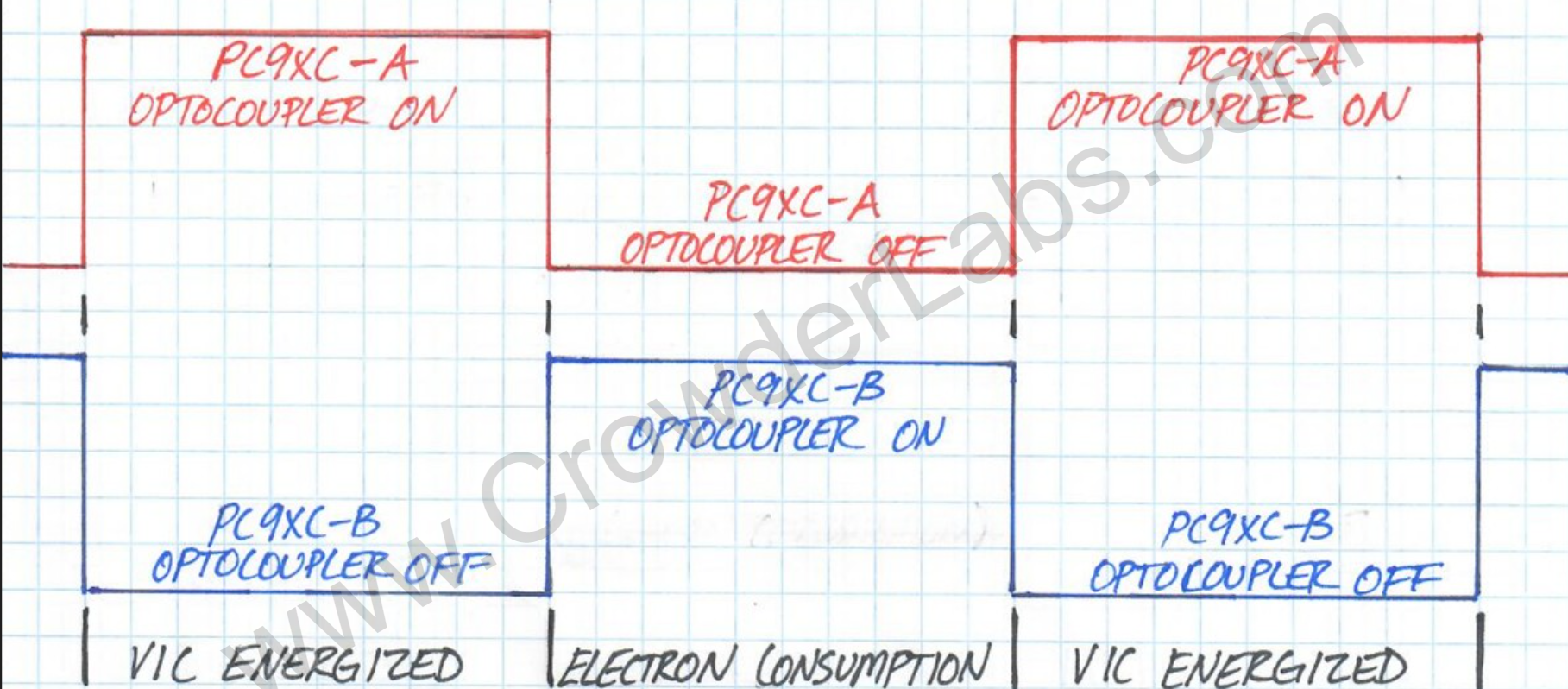
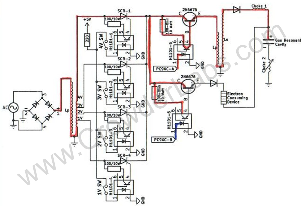
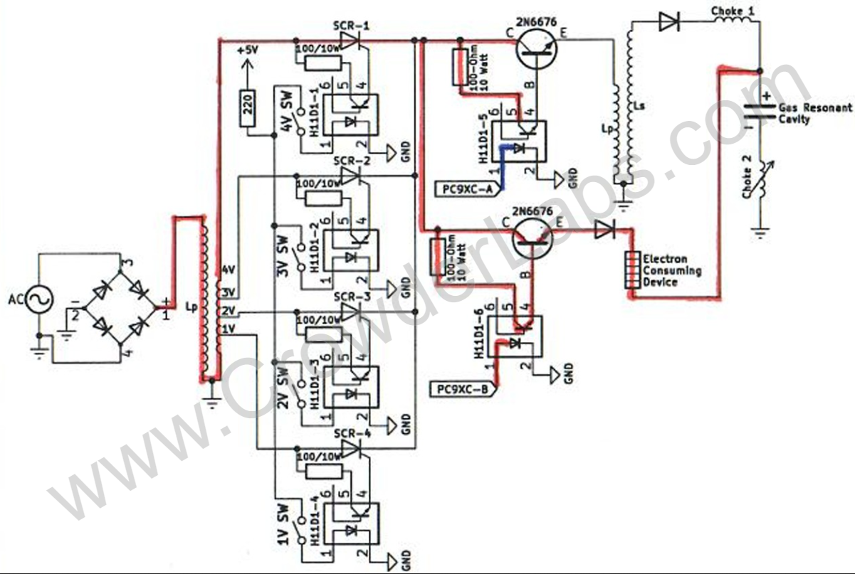
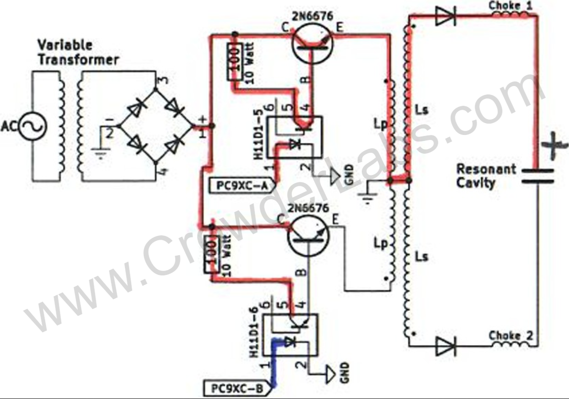
The schematic below illustrates the flip-flop switching application that facilitates electron extraction. Rectified mains supply provides a unipolar DC waveform that energizes the step-down transformer to produce a low voltage at a fixed frequency of 120Hz. Conversely, a filtering capacitance can allow a wider range of frequencies. Secondary coil taps in conjunction with switch-selected optocoupler triggered SCRs controls the voltage applied to the primary coil of the VIC step up stage (see page 79 for circuit board). The 120Hz has a superimposed gate signal via optocoupler “H11D1-5”, which is triggered via a PC9XC circuit. This optocoupler controls the number of pulses applied to the base of the power NPN. Diagram 3 details the waveform of this flip-flopping behavior.
The optocoupler “H11D1-6” is triggered 180o out of phase with respect to H11D1-5. During this time, positive potential is applied to one side of the electron consuming device. This causes liberated electrons within gas resonant cavity (see Gas Resonant Cavity / Hydrogen Gas Gun section for further details) to be attracted to this positive potential which leads to flow into electron consuming device.
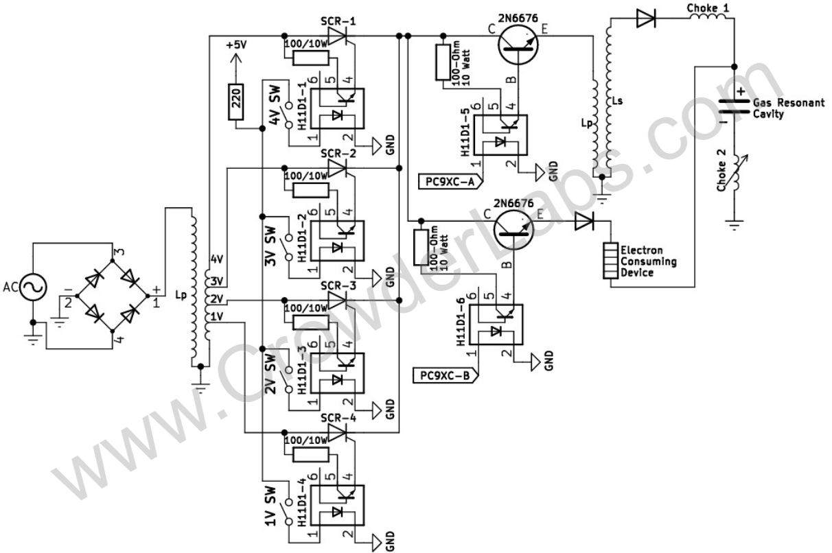
Diagram 3:
Electron Extraction Logical Flow - Phase 1:
Electron Extraction Logical Flow - Phase 2:
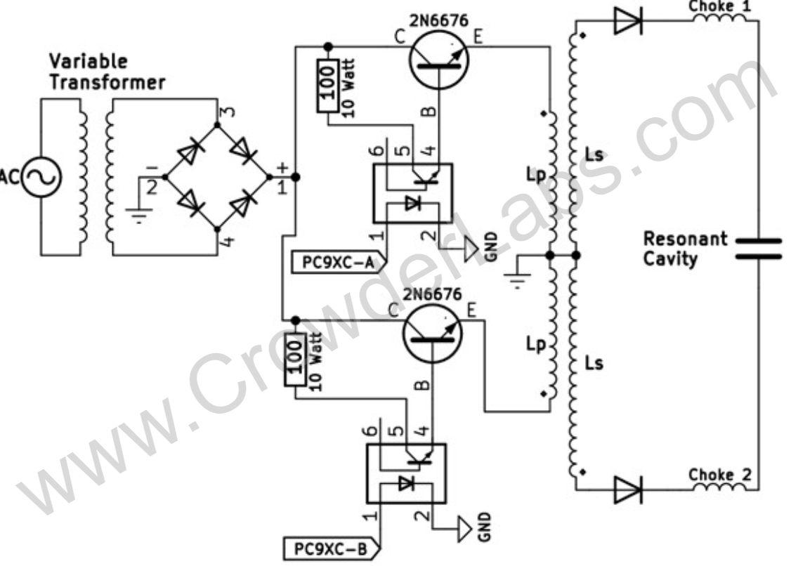
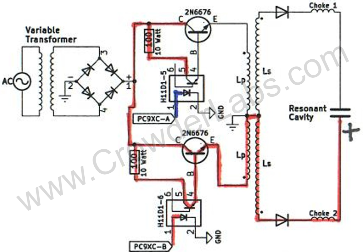
With reference to the schematic1 below, another application utilizing the flip-flopping action is illustrated for operation of the steam resonator. As shown in the aforementioned Diagram 3, the optocoupler signals, PC9XC-A and PC9XC-B are 180o out of phase with respect to one another. An adjustable rectified DC voltage is supplied, via the variable transformer, having a fixed frequency of 120Hz. During PC9XC-A triggering of the first power transistor, a unipolar rippling DC waveform is applied to the first primary coil, causing a high positive potential – via step-up transformer – to be applied to the first resonant charging choke coil, by forward biasing the series diode, onto the top plate of the resonant cavity structure. The bottom primary/secondary pair is opposite in polarity, reverse biasing the series diode, not permitting any potential to be applied to the second plate.
During PC9XC-B triggering of the second transistor, a unipolar rippling DC waveform is applied to the second primary coil, causing a higher positive potential – via step-up transformer - to be applied to the second resonant charging choke coil, by forward biasing the series diode, onto the bottom plate of the resonant cavity structure. At this time, the top primary/secondary pair is opposite in polarity, reverse biasing the series diode, not permitting any potential to be applied to the top plate.
It should be apparent, that applying a differential polarity is avoided. Only positive polarity is utilized in this arrangement, as only one pair of electrodes are present. This flip-flopping positive polarity influences the oxygen and hydrogen atoms, causing atomic/molecular flexing which produces heat energy.
Steam Resonator Logical Flow - Phase 1:
Steam Resonator Logical Flow - Phase 2:
Frequency is supplied by a PC9XB arrangement (see PC9XB analysis section for refresher) where an initial frequency is divided by multiples of ten and conditioned to have a 50% duty cycle. This circuit incorporates a frequency selection capability that is provided by a rotary switch, having the pole terminal interconnected to inputs 1,3,5,9,11,13 of the first hex inverter IC (74LS04-1). The input waveform polarity is inverted as shown in the scope shot below. Channel one (yellow) is representative of the pulse frequency into input pins. Channels 2, 3 and 4 (teal, magenta, dark blue) are representative of the three channels going out to optocoupler sets associated with this first hex inverter.
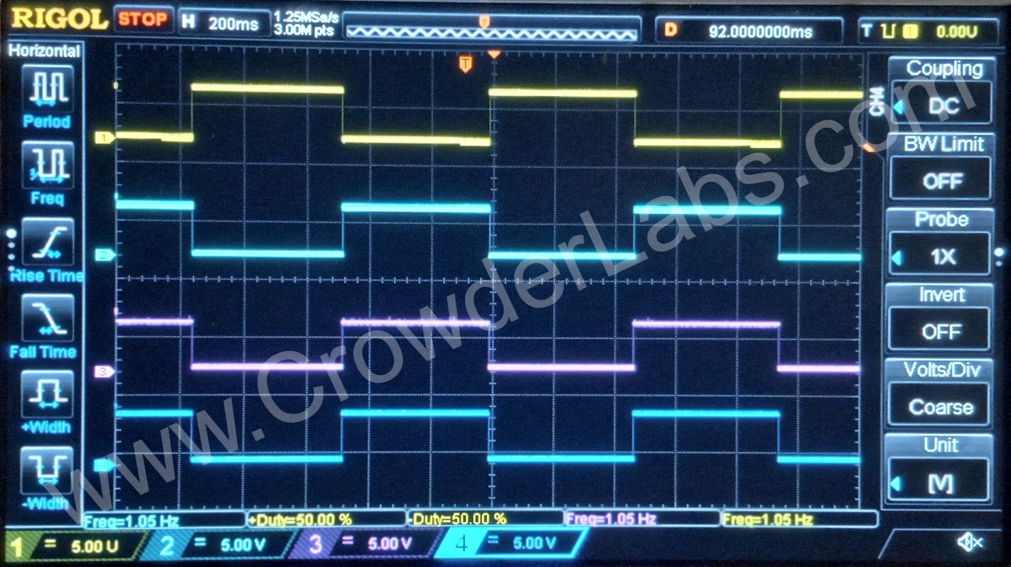
74LS04-1 output pin #2 has a 220Ω, ¼ watt resistor wired in series which triggers an externally mounted LED, indicating the inverter’s LOW logic level. 74LS04-2 output pin #2 has a 220Ω, ¼ watt resistor wired in series to provide a visual indication during the opposing logic state of the 74LS04-1. Output pins #8, #10, #12 of each inverter are connected to their respective optocouplers, each having a series 220Ω, ¼ watt cathode resistor to limit the current to 20mA. Optocouplers (H11D1-1, H11D1-2, H11D1-3) are all turned ON at the same time when 74LS04-1 is in a LOW logic state. During a HIGH logic state, these optocouplers are all turned OFF.
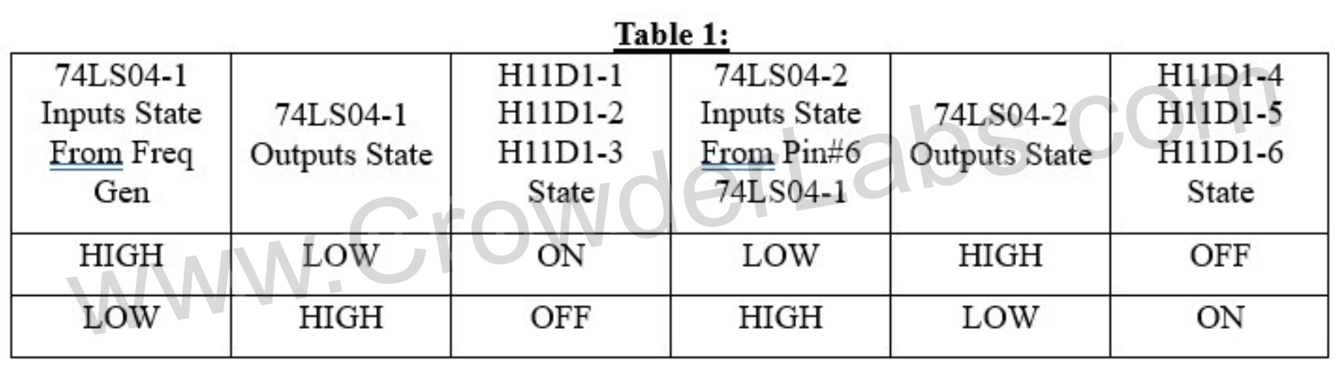
74LS04-1 output pin #6 is connected to the input pins #1, #3, #5, #9, #11, and #13 of the second hex inverter IC (74LS04-2). This produces a logical state that is inverse relative to 74LS04-1 but non-inverted relative to pulse frequency polarity (see logic chart below). Optocouplers (H11D1-4, H11D1-5, H11D1-6) are all triggered at the same time when 74LS04-2 is in a LOW logic state. During a HIGH logic state, these optocouplers are all turned OFF. Logic is summarized below in Table 1.
PC9XC Logical Flow - Phase 1:
PC9XC Logical Flow - Phase 2:
PC9XC - Variable Gate Circuit
Stan's Original Literature
PC9XD - Voltage Regulator Circuit
PC9XD - Voltage Regulator Circuit
Circuit Analysis
PC9XD - Voltage Regulator Circuit
Stan's Original Literature
PC9XE - Sequential Gate Card
PC9XE - Sequential Gate Card
My Circuit Analysis
YouTube video: PC9XE Sequential Gate Circuit
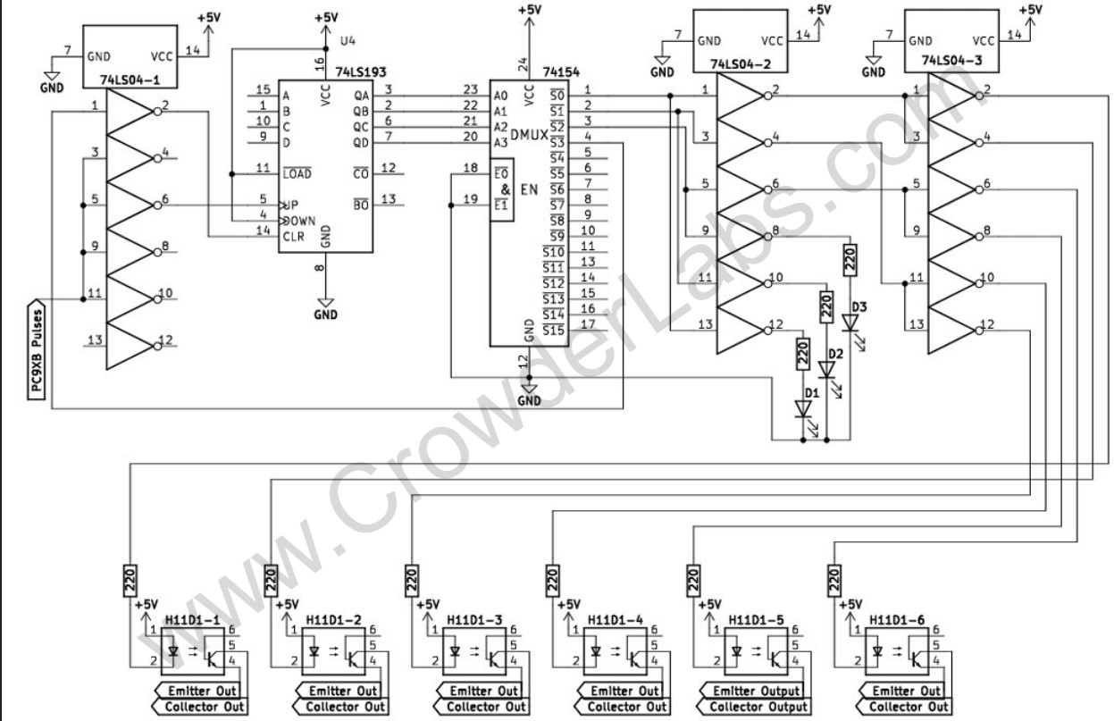
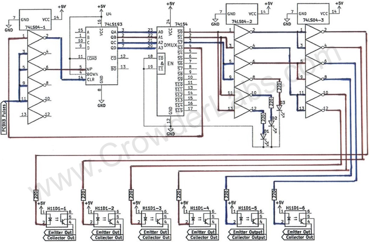
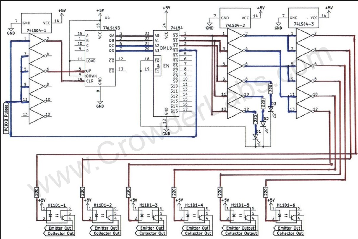
Schematic:
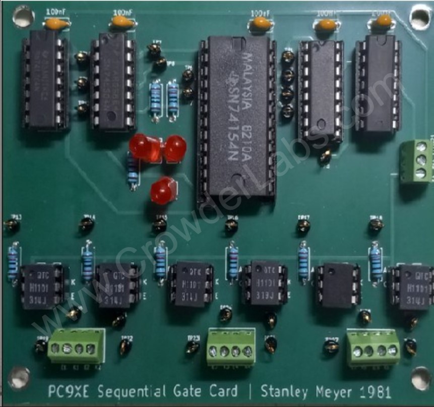
Replica PCB Top:
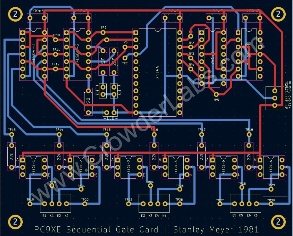
Replica PCB Traces:
Explanation:
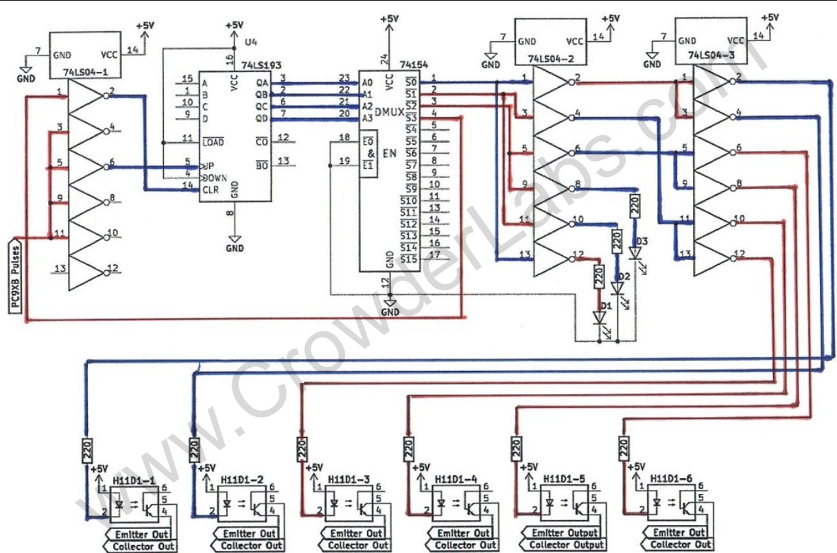
The circuit allows sequential selection of multiple circuit channels through opto-coupler isolation. The principle involves selecting and isolating a single pair of electrodes to avoid continuous application of power. Selection is possible between one to sixteen separate channels.
From the schematic below, the “optocoupler network” forms a triple AND circuit. First, the PC9XB frequency generator provides a 50% duty cycle square wave of a desired frequency to obtain resonance. Second, the PC9XC variable gate (with a fixed 50% duty cycle frequency) provides a gating function that performs, variability of how many pulses are permitted to be applied to transistor base. Third, the PC9XE sequentially completes the circuit, behaving as a solid-state switch to permit gated waveform to be applied to power transistor base. The power transistor is an NPN type, in a high side switching arrangement. Two models are referenced: 2N6676: 300v @ 15A / 2N6496: 110v @ 15A. Given the voltage ratings, input voltage could range from 110v to 240v.
Binary Counter - 74193:
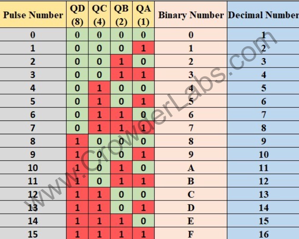
The 4-bit binary counter, shown in below, can perform counting-up (pin #5) and counting-down (pin #4) functions. Counting up/down is accomplished when LOW to HIGH pulse edge is applied to the respective pin. The direction of count (up/down) is determined by which count input is pulsed while the other is held HIGH. In Stan’s application, a counting-up arrangement was used. Figure 28 shows the DOWN (pin #4) attached to the voltage supply (pin #16) to maintain a constant HIGH state for counting-up operation. LOAD (pin #11) is attached to voltage supply to inhibit this function, as no loading of inputs is performed during circuit operation.
CLEAR (pin #14) is utilized to force all the four outputs to a LOW logic state when a HIGH logic state is applied. Clearing is independent of the count and load inputs. This means that at any point in counting, if the CLEAR function is triggered, the outputs will be reset to all LOW (0) and counting will start at the beginning (0000). Each count-up pulse applied will cause the four binary outputs (QA, QB, QC, QD) to increment in an increasing binary count order. Counting will increment from 0 to 15 (1-16 in decimal). When exceeding 15 (“F”) occurs, the CARRY OVER (pin #12) produces a pulse equal in width to the count pulse. In certain applications, this pulse can be used to return the counter back to starting at 0. Table 2 provides a functional overview of the binary counter operation.
74193 Logic Table:
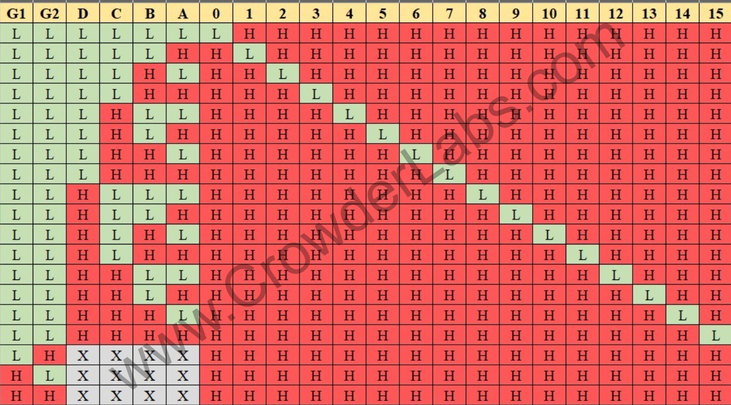
74154 Demultiplexer Operation:
In simple terms, this model of demultiplexer (DMUX), as shown in Figure 29 below, is an integrated circuit capable of up to 16 channel selections through what is known as decoding. Channel selections only occur one at a time. The channel selected is dependent upon the binary values at the four inputs (pins #23, #22, #21, #20). All output channels are at a resting logic state of HIGH (1). When a channel is selected, the logic state changes to LOW (0). Two enable pins (pins #18, #19) must be kept at a LOW logic level in order for chip to operate. This will be understood shortly. The frequency of binary value inputs determines how fast the output channels are selected.

Shown in the table below, the function table showing the correlation between the binary input values (A=#23, B=#22, C=#21, D=#20). A logical state of LOW (0) is represented by “L”. A logical state of HIGH (1) is represented by “H”. It can be seen that the two enable pins (G1, G2) are kept LOW through the channel selection process.
74154 Logic Table:
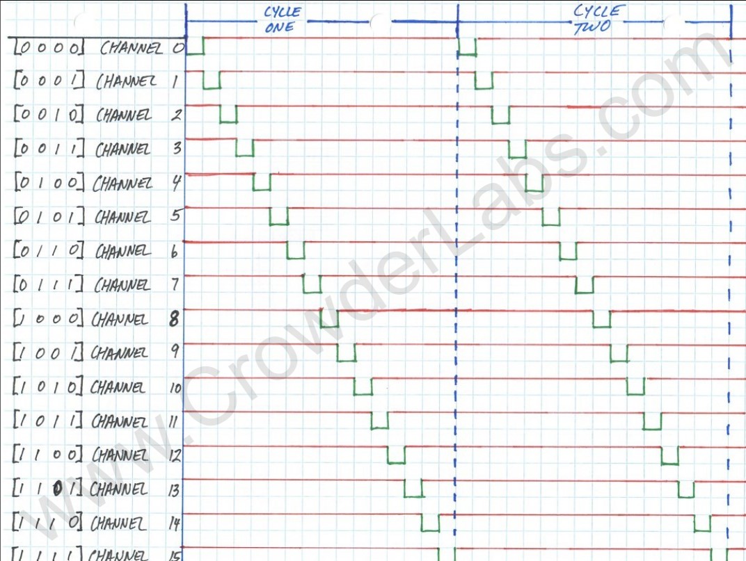
The diagram below illustrates a representation of what a digital analysis would show for all sixteen channels during operation. Binary value at the input pins is located at the far left, with corresponding channel selection. The last channel could be used to trigger the clear pin on the driving binary counter for certain applications.
74154 Waveform Diagram:
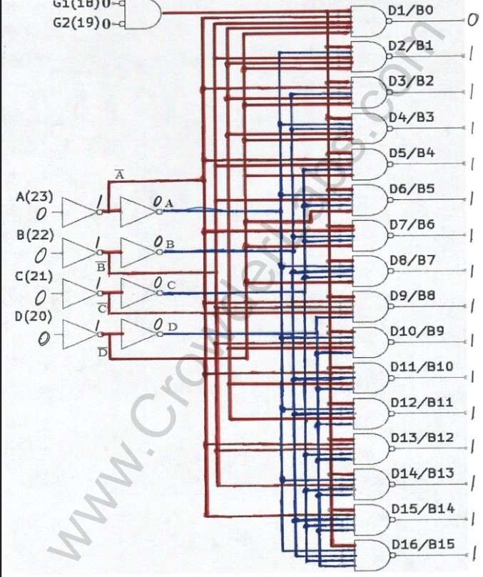
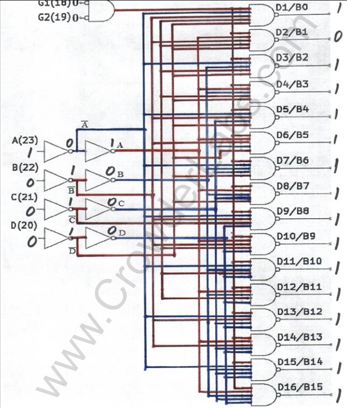
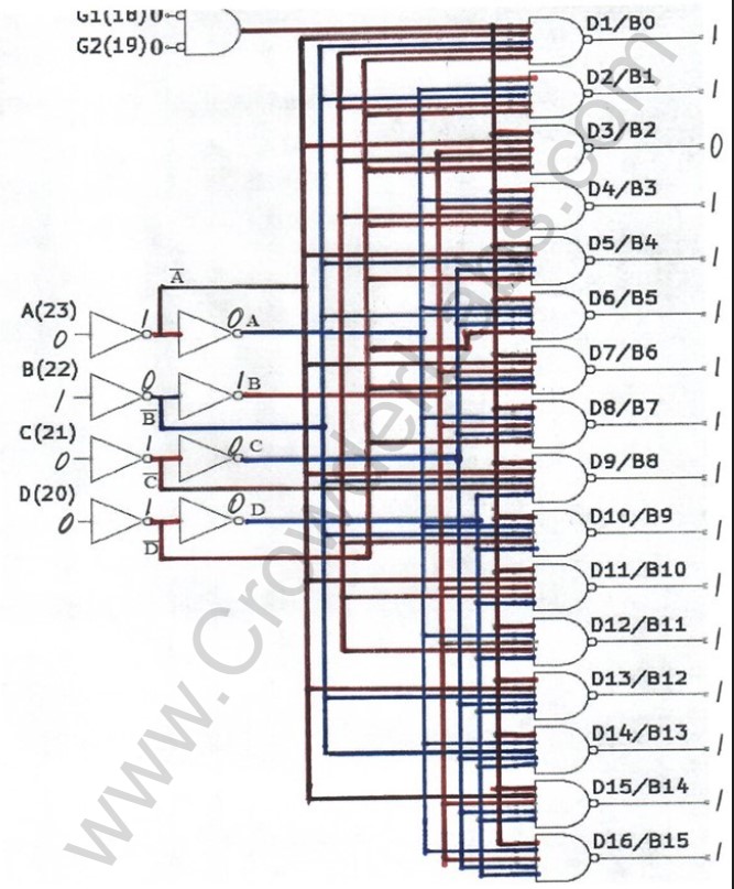
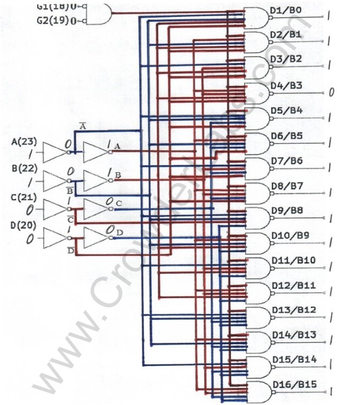
Internally, the 74154 is composed of two stages of four inverters at the binary inputs. The first stage changes the LOW (0) logic into HIGH (1) logic. Second stage of inverters re-invert the HIGH (1) logic back to LOW (0) logic states. These work in conjunction with a network of NAND logic gates to control the selection of each output channel. Both enable inputs (G1/G2) are connected to ground (0V), being inverted before entering their associated AND logic gate. This arrangement produces a constant HIGH logic state to one input of each of the sixteen NAND gates (as seen by the red lines). None of the channels are available for selection without G1 and G2 being maintained LOW.
Within the next four sections, the internal operations for each channel selection are provided. The red lines are indicative of the circuits associated HIGH (1) logic states. The blue lines are indicative of the circuits associated with LOW (0) logic states.
74154 Sequence 1 - Selecting Binary Channel "0"/Decimal Channel "1":
74154 Sequence 2 - Selecting Binary Channel "1"/Decimal Channel "2":
74154 Sequence 3 - Selecting Binary Channel "2"/Decimal Channel "3":
74154 Sequence 4 - Selecting Binary Channel "3"/Decimal Channel "4":
Triple Stack Sequencing Schematic:
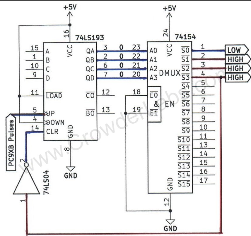
74193 & 74154 - Sequence 1:
As the binary counter increments, corresponding binary values are sent over the four lines as shown below. Initial state of 0000, after clear has been triggered, causing the 74154’s S0 (Channel “1”) to change from a HIGH state to LOW state as shown below.
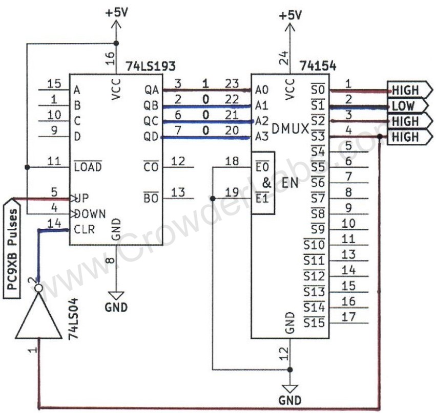
74193 & 74154 - Sequence 2:
A LOW to HIGH pulse (Pulse #1) received from the 9XB, incrementing the 74193 to a binary value of “1” (0001). This output state causes the 74154’s S1 (Channel “2”) to change from a HIGH to LOW state. Previous S0 (Channel “1”) returns back to HIGH state as shown below.
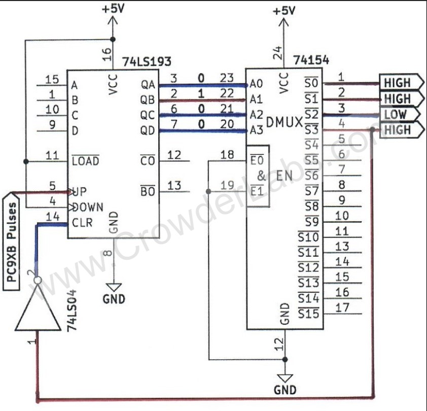
74193 & 74154 - Sequence 3:
Another LOW to HIGH pulse (Pulse #2) is received from the 9XB, incrementing the 74193 to a binary value of “2” (0010). This causes the DMUX’s output S2 (Channel “3”) to change from a resting HIGH state to LOW state. Previous S1 (Channel “2”) changes back to HIGH from triggered LOW state as shown below.
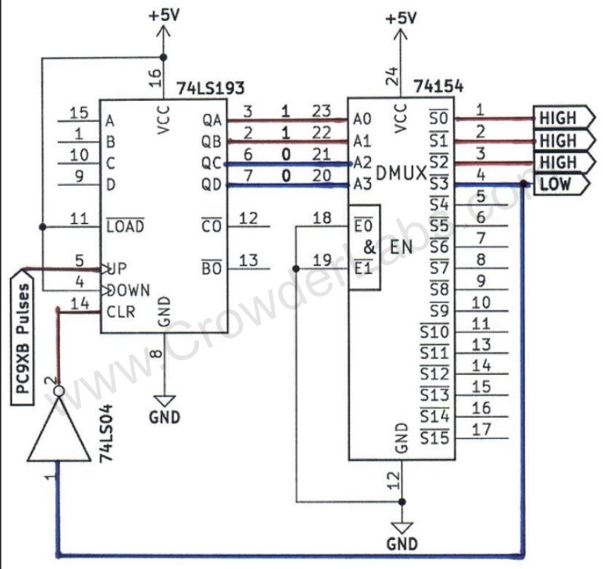
74193 & 74154 - Sequence 4:
Finally, a LOW to HIGH pulse (Pulse #3) is received from the 9XB, Incrementing the 74193 to a binary value of “3” (0011). This causes DMUX’s S3 (Channel “4”) to change from resting HIGH state to LOW state. Previous S2 (Channel “3”) returns to HIGH state from triggered LOW state as shown below.
PC9XB Pulses into hex Inverter:
Pulse train (from PC9XB) is applied into the first hex inverter (74LS04-1) input pins #3, #5, #9, and #11. Duty cycle is a fixed at 50%. The screenshot below is provided to demonstrate the relationship between the input pulse train (Yellow), inverter input (pin #11 - Blue) and inverter output (pin #6 - Magenta).
Pulses into "COUNT UP" pin of 74193:
Output pin #6 increments the COUNT UP (pin #5) of binary counter (74LS193) by providing a HIGH logic state from the pulse frequency during its LOW logic state. The screenshot below shows the clock pulse applied to pin #5.
Binary bus count between 74193 & 74154:
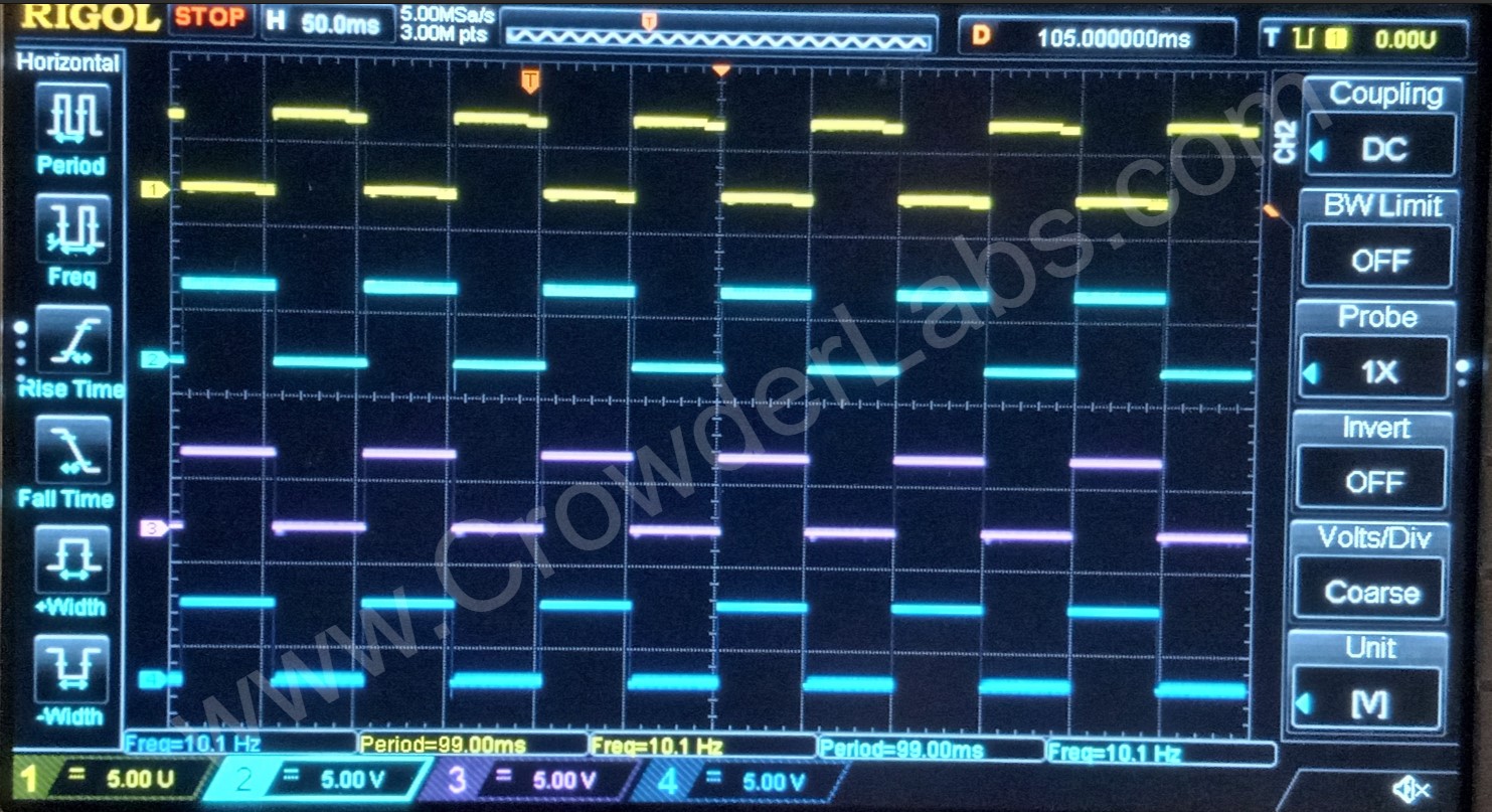
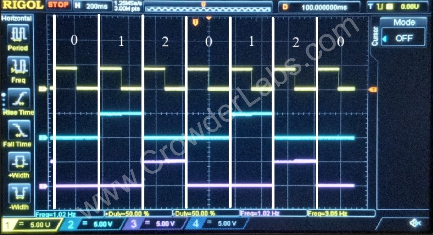
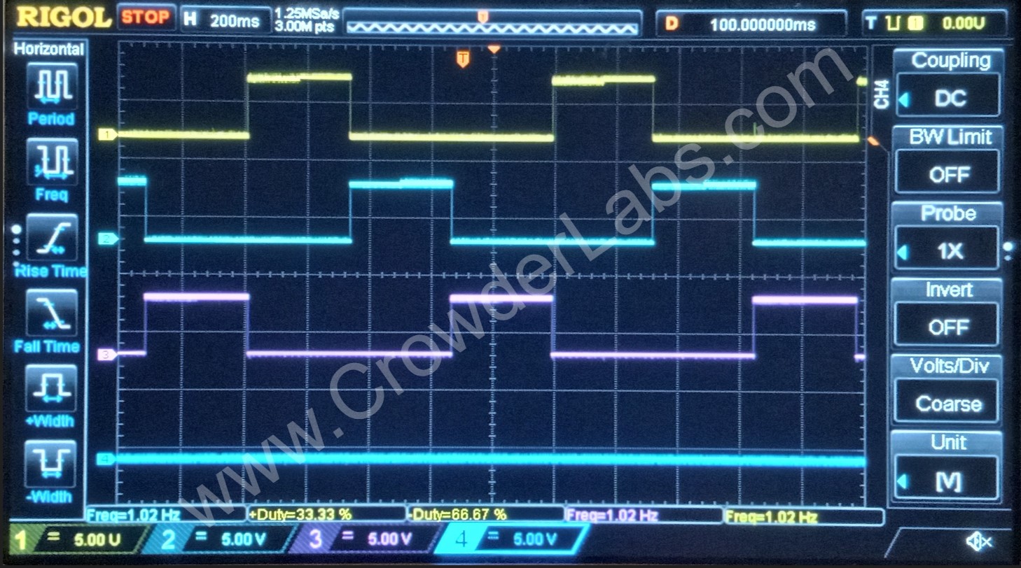
Pins #4, #11 on the 74193 are connected to (pin #16) to maintain a HIGH logic state. Due to LOAD and COUNT DOWN not being used, a HIGH logic state is maintained for operation. Binary output pins (#3[QA], #2[QB], #6[QC], and #7[QD]) count through a 4-bit binary sequence (0-3) for every low to rising edge of clock. In the screenshot below, the counting sequence is shown. Count values are divided by the white vertical lines. The counter is only counting to binary 2 (decimal “3”) with a reset on binary 3 (decimal “4”). Therefore, only two channels are utilized. Binary output [QA] is represented by the blue trace. Output [QB] is represented by the magenta trace.
Output channels of 74154:
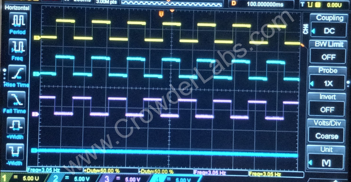
Outputs from the binary counter are communicated to the inputs of the DMUX (pin #23[A0], #22[A1], #21[A2] and #20[A3]). These cause the DMUX to select corresponding channels (pin #0[CH1], #1[CH2], and #2[CH3], #3[CH4]). When a corresponding channel is triggered, its logical state changes from a resting HIGH to LOW. Four outputs are selected in a sequential fashion. The screenshot below, illustrates the sequential manner of each channel. The first channel is represented by the yellow trace. The second channel is represented by the blue trace. The third channel is represented by the magenta trace. Finally, the fourth channel is represented by the dark blue trace, which is LOW due to being reset signal for binary counter.
74154 output channels through first hex inverter:
The screenshot below, shows the inversion of each 74154 channel, after passing through the second hex inverter (74LS04-2). Channel 1 is connected to input pins #1 and #13. Channel 2 is connected to input pins #3 and #11. Channel 3 is connected to input pins #5 and #9. All inputs are at a LOW logic state. Output pins #8, #10 and #12 are connected to the anode of an LED through a series resistor of 220Ω. These LEDs provide visual indication of what channel is currently on when corresponding output is in a HIGH logic state. Each LED has a 20mA current through it [5v / 220Ω = 0.020A (20mA)].
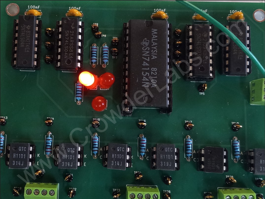
LED - Sequence 1:
Below shows the first LED illuminated, which represents output “0” (Pin #1) of the DMUX.
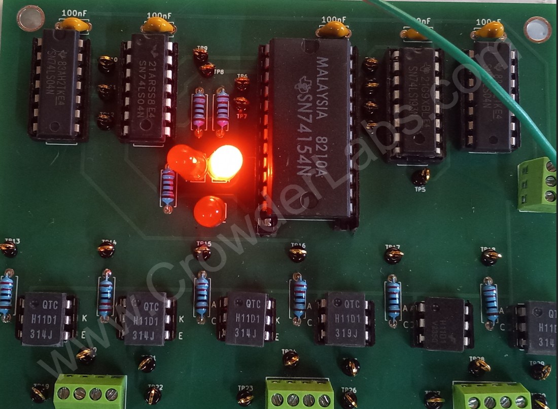
LED - Sequence 2:
Below shows the second LED illuminated, which represents output “1” (Pin #2) of the DMUX.
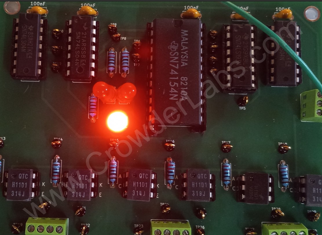
LED - Sequence 3:
Below shows the third LED illuminated, which represents output “2” (Pin #3) of the DMUX.
74154 output channels through second hex inverter:
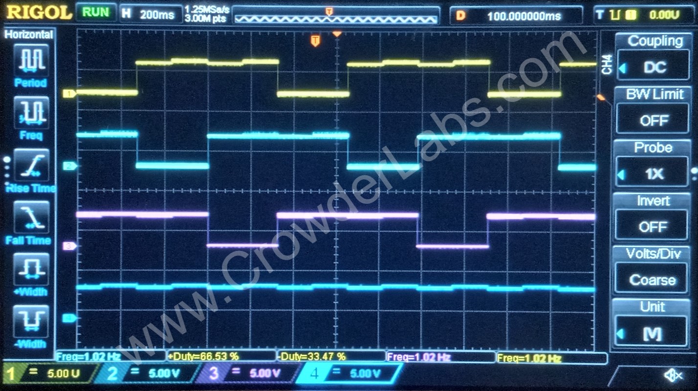
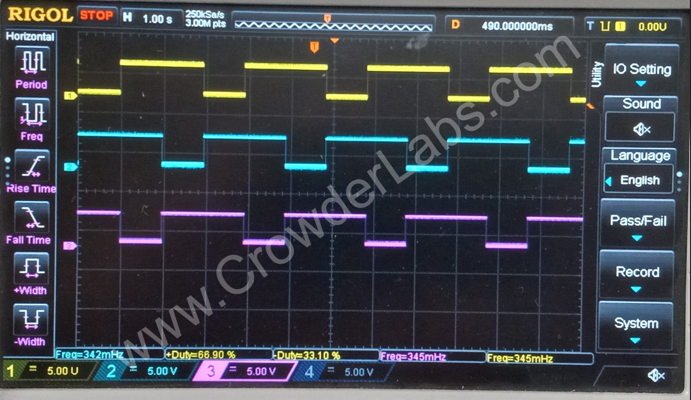
The second hex inverter, 74LS04-2, output pins: #2, #4, and #6 are connected to paired inputs on the third hex inverter 74LS04-3. The screenshot below shows the waveforms communicated to each pair of H11D1 associated with outputs from this third hex inverter. Yellow trace shows sequence 1 (binary 0) which triggers H11D1-1 and H11D1-2 via 74LS04-3 output pins #2 and #4. Teal trace shows sequence 2 (binary 1) which triggers H11D1-3 and H11D1-4 via 74LS04-3 output pins #10 and #12. Magenta trace shows sequence 3 (binary 2) which triggers H11D1-5 and H11D1-6 via 74LS04-3 pins #6 and #8. A sequential order has been maintained.
System Logic Table:
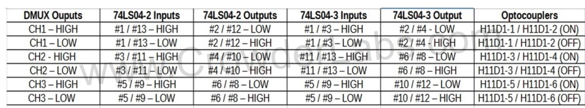
The output pins produce a LOW logic state. This LOW logic pulls down on the optocoupler cathode, turning on the internal LED. When outputs are in a HIGH logic state, the internal LED becomes reversed bias, thus keeping the LED off. The use of optocouplers provides isolation between the control circuitry and the optocoupler outputs. In simple terms, an optocoupler is a light triggered bipolar junction transistor (BJT). When the LED is turned on, the light sensitive base of the BJT causes the Collector/Emitter to come into conduction, performing the function of a switch. The amount of current conducted is related to the Current Transfer Ratio (CTR) of the optocoupler. This is similar to the gain of a regular BJT but measured as a ratio of the output current to the input current. For the H11D1, this is 20% on average. The collector and emitter of each optocoupler are connected to individual pins to allow external circuit connections. The table below details the logic continuity from the DMUX, through the hex inverters, to the optocouplers:
Logical Flow - Phase 1:
Logical Flow - Phase 2:
Logical Flow - Phase 3:
Logical Flow - Phase 4:
PC9XE - Sequential Gate Card