3D Printable Photon Injected Resonant Cavity
Stan had a "triple stack" which was composed of three individual resonant cavities stacked on top one another. These were large and made of machined Delrin. At the top of each was a circular PCB composed of 5mm 660nm LEDs. 660nm LEDs were seen throughout Meyer's technology. In an effort to miniaturize, and ease investigations for such, I have designed a version that uses the tube dimensions of the small resonant cavities.
FINISHED ASSEMBLY:
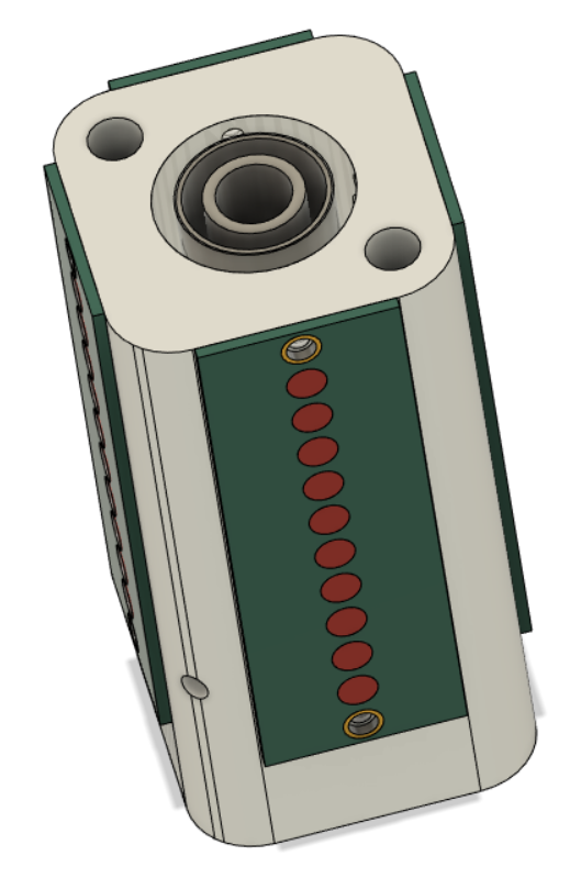
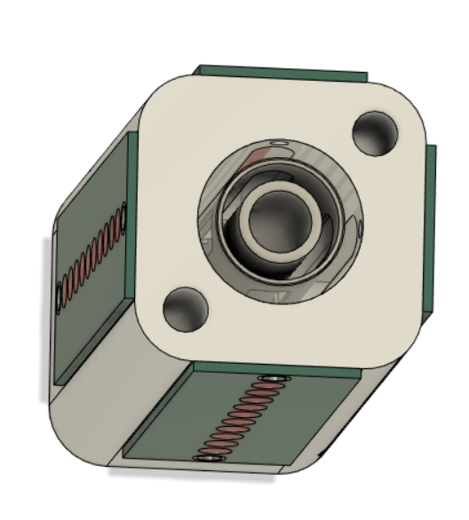
Body of the unit. Received 4 LED PCBs at a 90 degree displacement around the periphery. Internal has an acrylic "lens", 0.75" outer electrode, and 0.50" inner electrode coaxially placed relative to one another. Two 1/4" holes are 180 degrees displaced relative to one another for mounting via nylon all thread rod. Hole for connections to the internal tubes are provided (on seen here for 0.75") on the side. Also, using a new method, at the bottom of the body for the inner electrode (see at bottom).
Photon Injected Resonant Cavity Body.stl
INNER ELECTRODE:
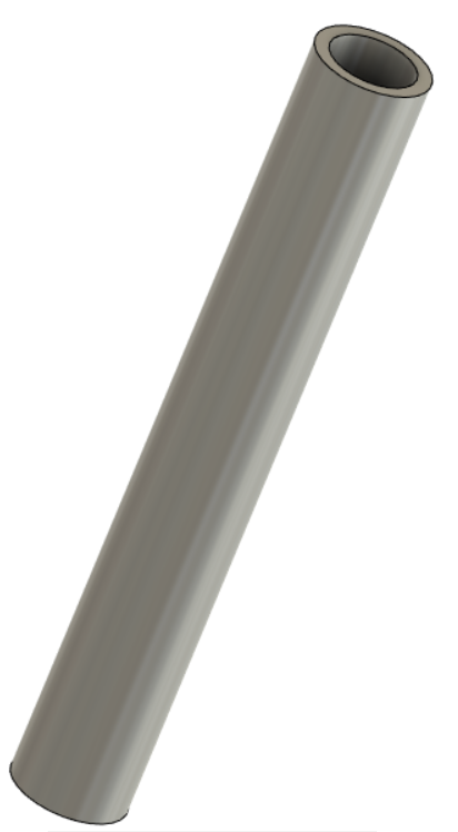
1/2" (0.500") outside diameter. 3.50" long. T-304 stainless steel tube. 0.060" wall.
OUTER ELECTRODE:
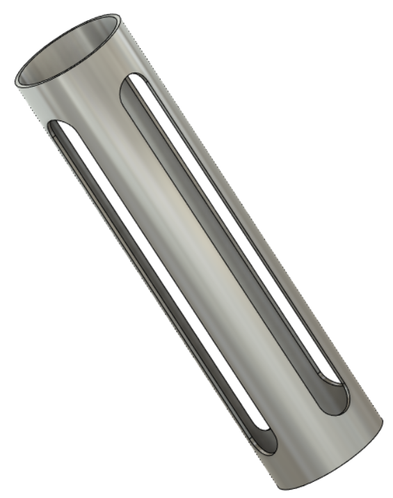
3/4" (0.75") outside diameter. 3.00" long. T-304 stainless steel. 0.035" wall. Machining these slots can become pricey. Therefor, a stencil that slides over the electrode can be used to manually mark the area for the grooves and cut them out in an alternative fashion.
ACRYLIC LENS:
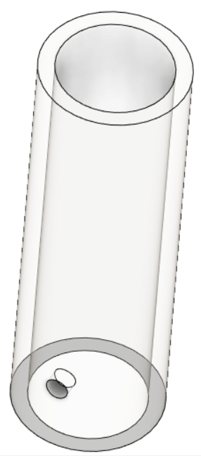
Acrylic lens is made from casting resin. This below would be finished product. Included is the hole for connecting to 3/4" electrode from outside. STL would be template for making a master mold.
LED PCB:
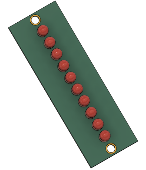
Representation of a PCB manufactured. Composed of 10 660nm - 5mm LEDs.
TOP VIEW:

