My Circuit Analysis
YouTube video: PC9XE Sequential Gate Circuit
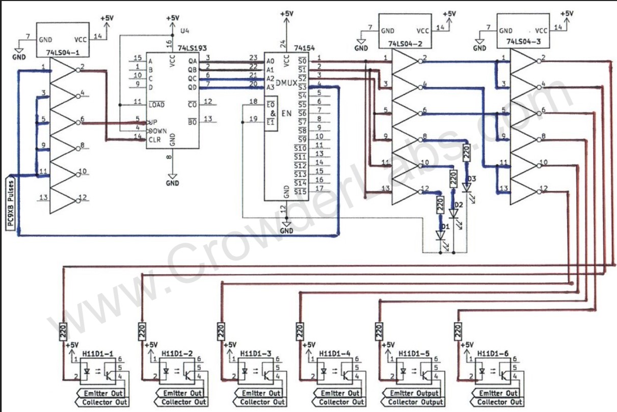
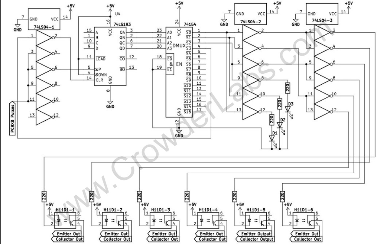
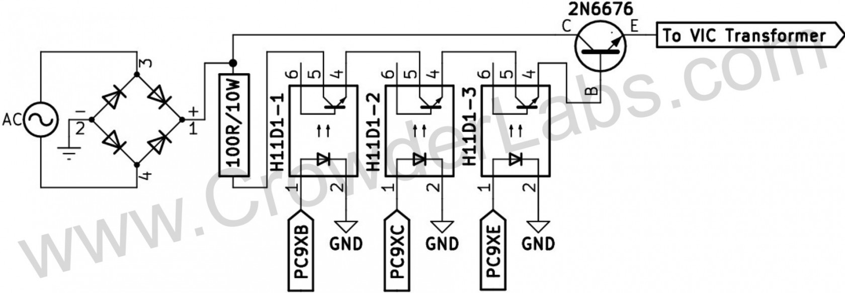
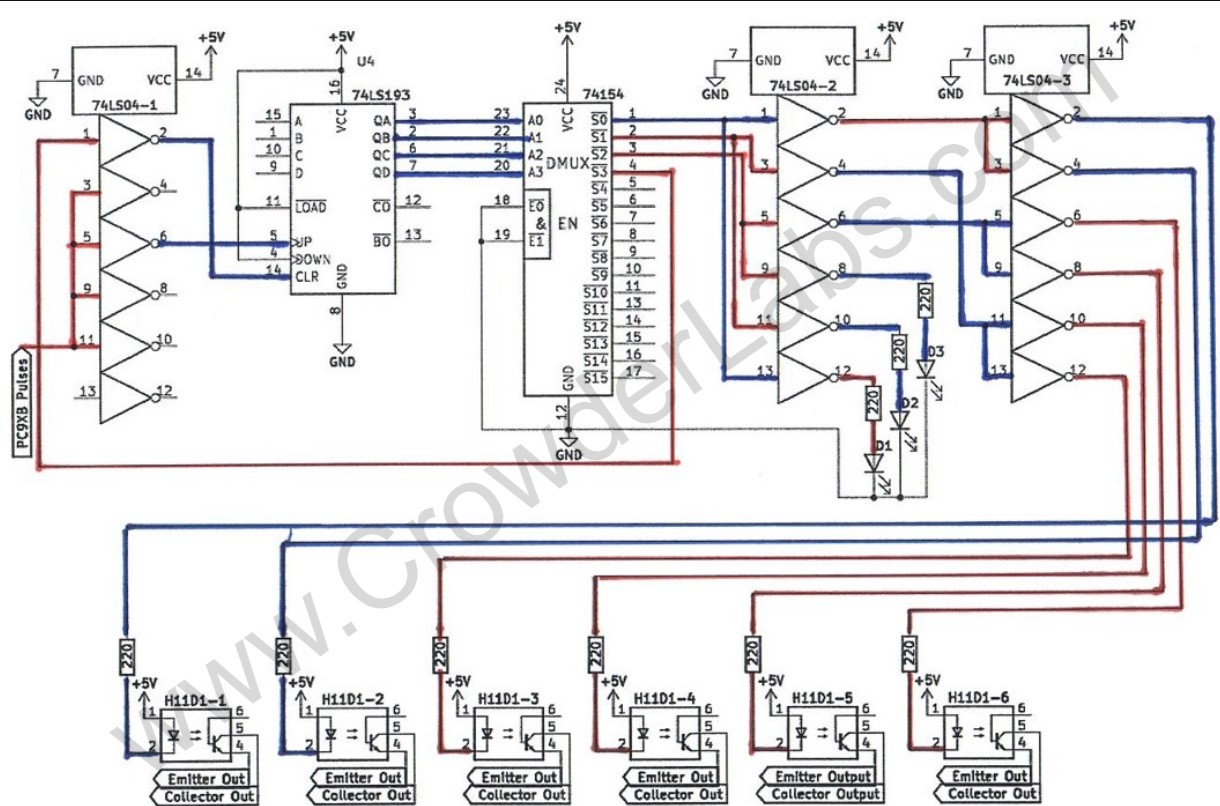
Schematic:

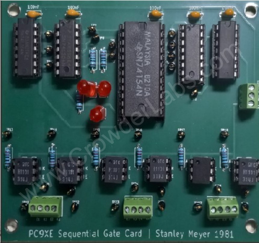
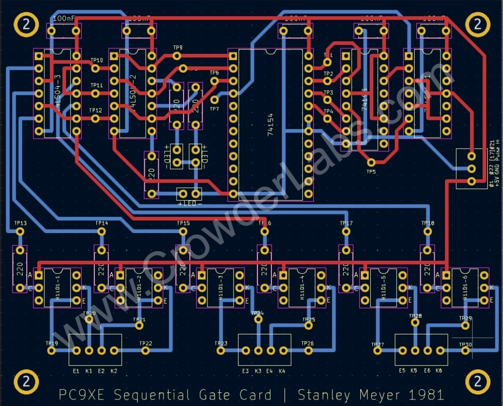
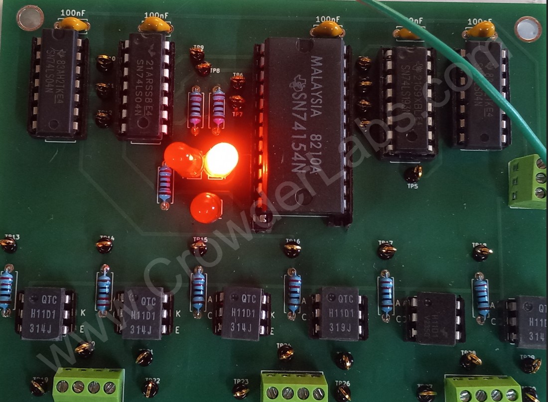
Replica PCB Top:

Replica PCB Traces:

Explanation:
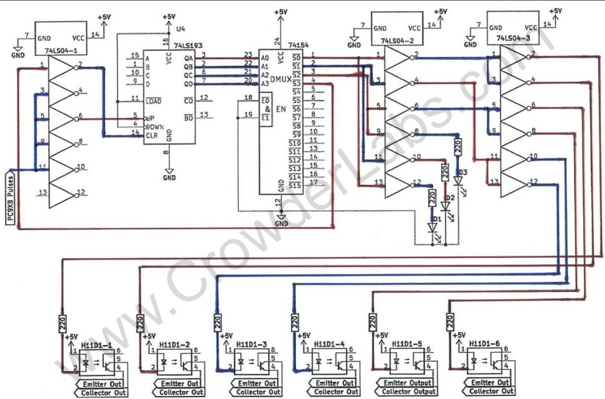
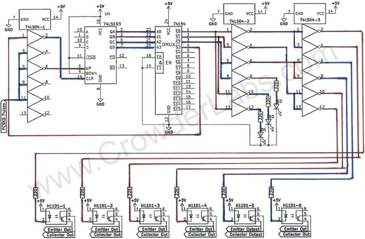
The circuit allows sequential selection of multiple circuit channels through opto-coupler isolation. The principle involves selecting and isolating a single pair of electrodes to avoid continuous application of power. Selection is possible between one to sixteen separate channels.
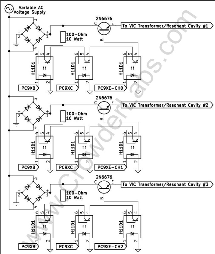
From the schematic below, the “optocoupler network” forms a triple AND circuit. First, the PC9XB frequency generator provides a 50% duty cycle square wave of a desired frequency to obtain resonance. Second, the PC9XC variable gate (with a fixed 50% duty cycle frequency) provides a gating function that performs, variability of how many pulses are permitted to be applied to transistor base. Third, the PC9XE sequentially completes the circuit, behaving as a solid-state switch to permit gated waveform to be applied to power transistor base. The power transistor is an NPN type, in a high side switching arrangement. Two models are referenced: 2N6676: 300v @ 15A / 2N6496: 110v @ 15A. Given the voltage ratings, input voltage could range from 110v to 240v.

Binary Counter - 74193:
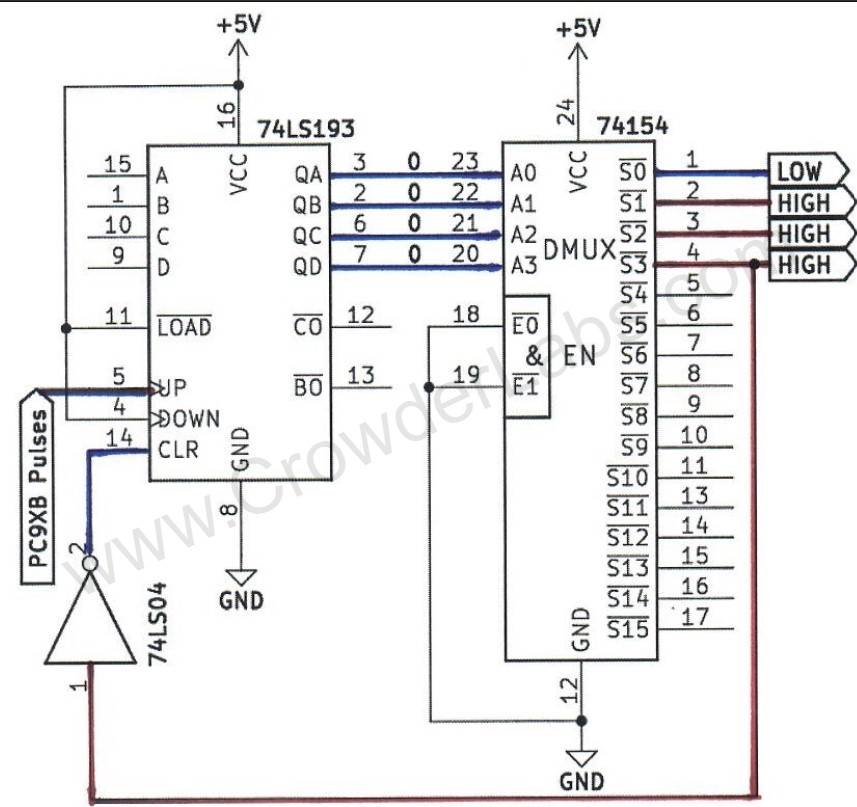
The 4-bit binary counter, shown in below, can perform counting-up (pin #5) and counting-down (pin #4) functions. Counting up/down is accomplished when LOW to HIGH pulse edge is applied to the respective pin. The direction of count (up/down) is determined by which count input is pulsed while the other is held HIGH. In Stan’s application, a counting-up arrangement was used. Figure 28 shows the DOWN (pin #4) attached to the voltage supply (pin #16) to maintain a constant HIGH state for counting-up operation. LOAD (pin #11) is attached to voltage supply to inhibit this function, as no loading of inputs is performed during circuit operation.
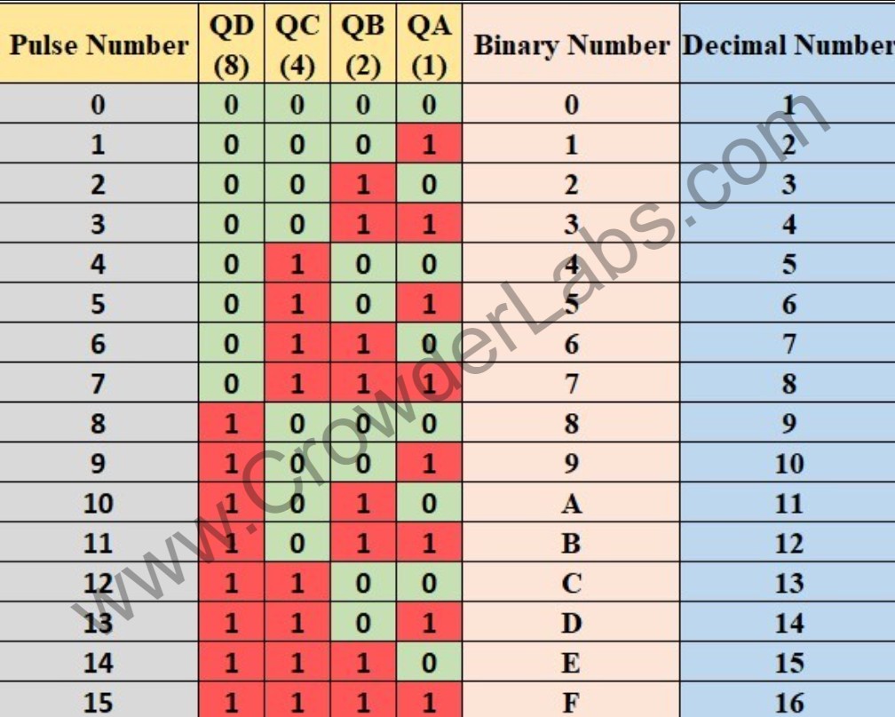
CLEAR (pin #14) is utilized to force all the four outputs to a LOW logic state when a HIGH logic state is applied. Clearing is independent of the count and load inputs. This means that at any point in counting, if the CLEAR function is triggered, the outputs will be reset to all LOW (0) and counting will start at the beginning (0000). Each count-up pulse applied will cause the four binary outputs (QA, QB, QC, QD) to increment in an increasing binary count order. Counting will increment from 0 to 15 (1-16 in decimal). When exceeding 15 (“F”) occurs, the CARRY OVER (pin #12) produces a pulse equal in width to the count pulse. In certain applications, this pulse can be used to return the counter back to starting at 0. Table 2 provides a functional overview of the binary counter operation.
74193 Logic Table:

74154 Demultiplexer Operation:
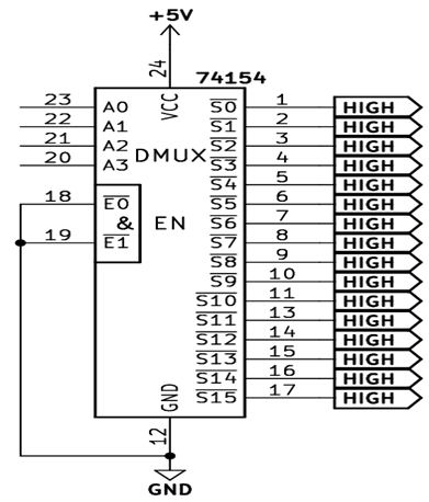
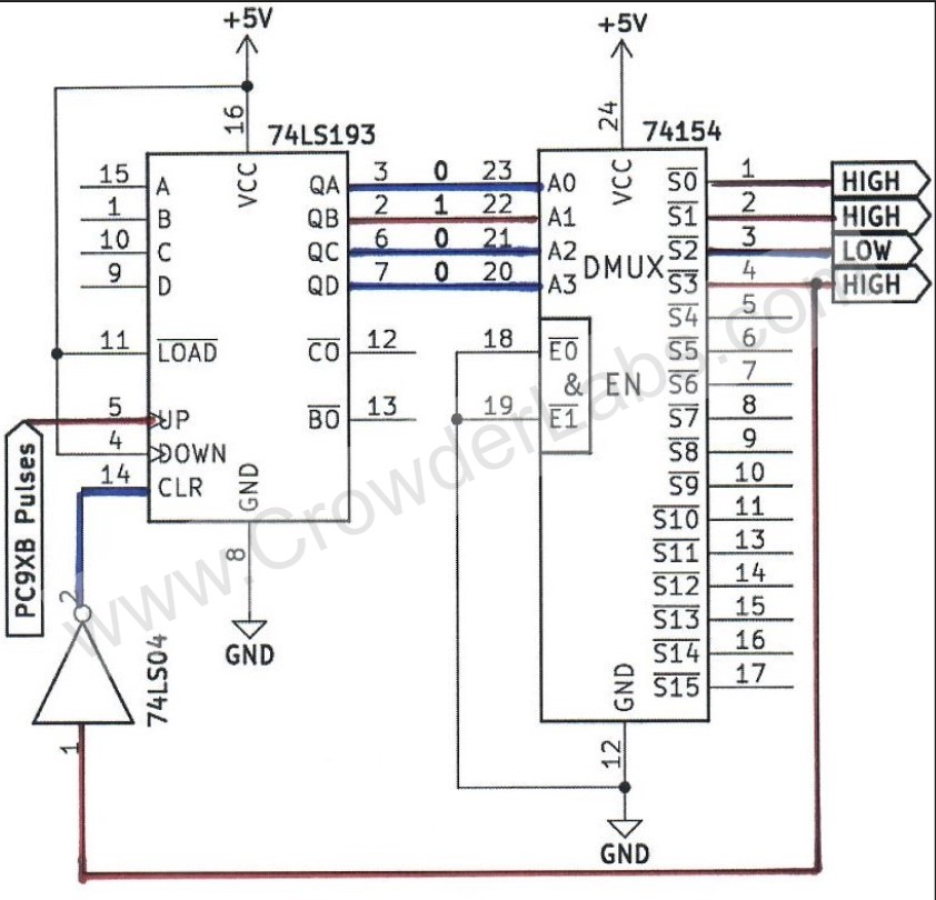
In simple terms, this model of demultiplexer (DMUX), as shown in Figure 29 below, is an integrated circuit capable of up to 16 channel selections through what is known as decoding. Channel selections only occur one at a time. The channel selected is dependent upon the binary values at the four inputs (pins #23, #22, #21, #20). All output channels are at a resting logic state of HIGH (1). When a channel is selected, the logic state changes to LOW (0). Two enable pins (pins #18, #19) must be kept at a LOW logic level in order for chip to operate. This will be understood shortly. The frequency of binary value inputs determines how fast the output channels are selected.

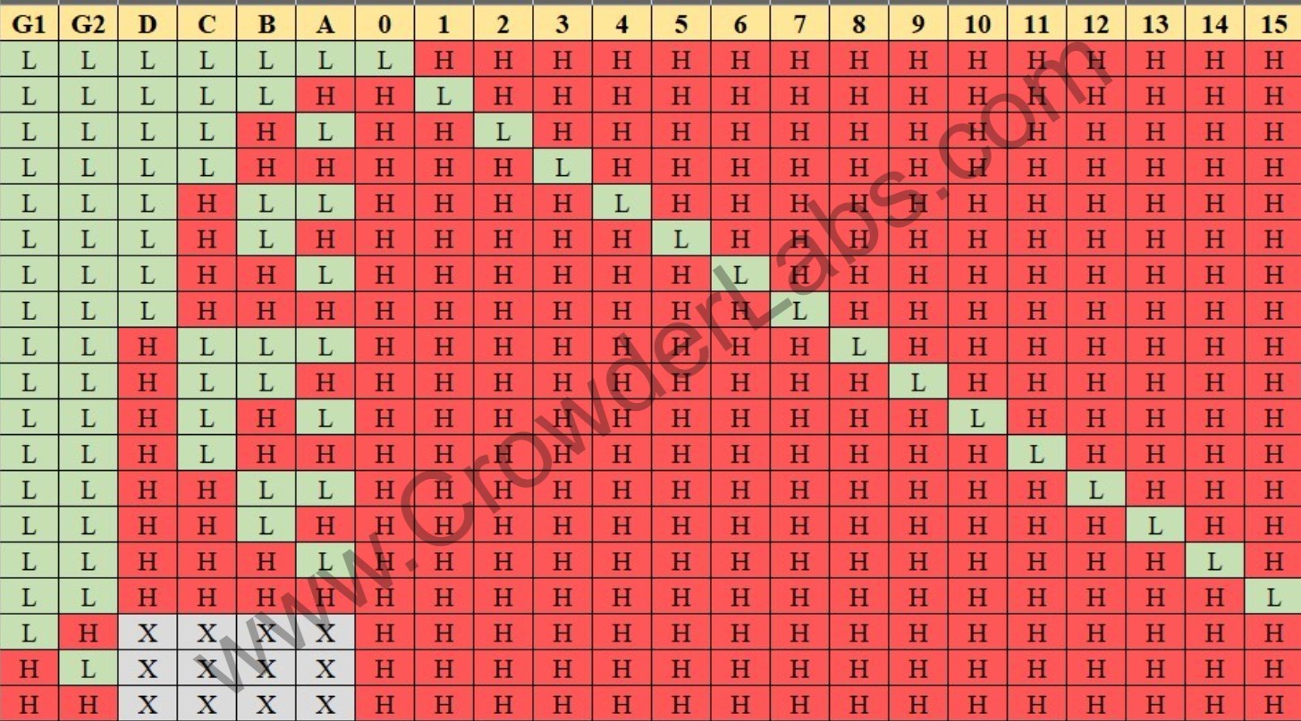
Shown in the table below, the function table showing the correlation between the binary input values (A=#23, B=#22, C=#21, D=#20). A logical state of LOW (0) is represented by “L”. A logical state of HIGH (1) is represented by “H”. It can be seen that the two enable pins (G1, G2) are kept LOW through the channel selection process.
74154 Logic Table:

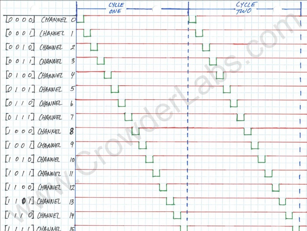
The diagram below illustrates a representation of what a digital analysis would show for all sixteen channels during operation. Binary value at the input pins is located at the far left, with corresponding channel selection. The last channel could be used to trigger the clear pin on the driving binary counter for certain applications.

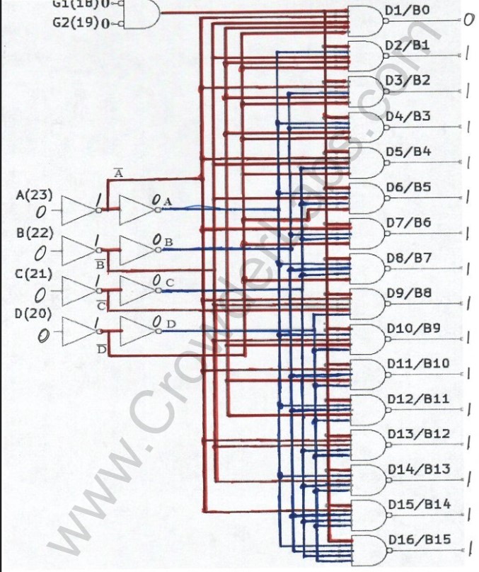
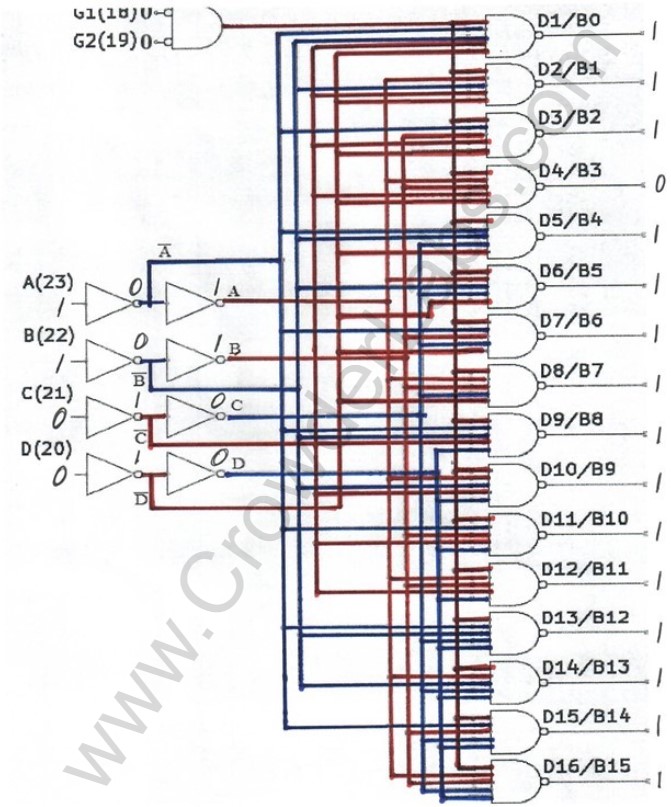
Internally, the 74154 is composed of two stages of four inverters at the binary inputs. The first stage changes the LOW (0) logic into HIGH (1) logic. Second stage of inverters re-invert the HIGH (1) logic back to LOW (0) logic states. These work in conjunction with a network of NAND logic gates to control the selection of each output channel. Both enable inputs (G1/G2) are connected to ground (0V), being inverted before entering their associated AND logic gate. This arrangement produces a constant HIGH logic state to one input of each of the sixteen NAND gates (as seen by the red lines). None of the channels are available for selection without G1 and G2 being maintained LOW.
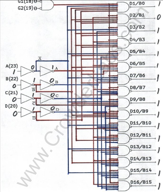
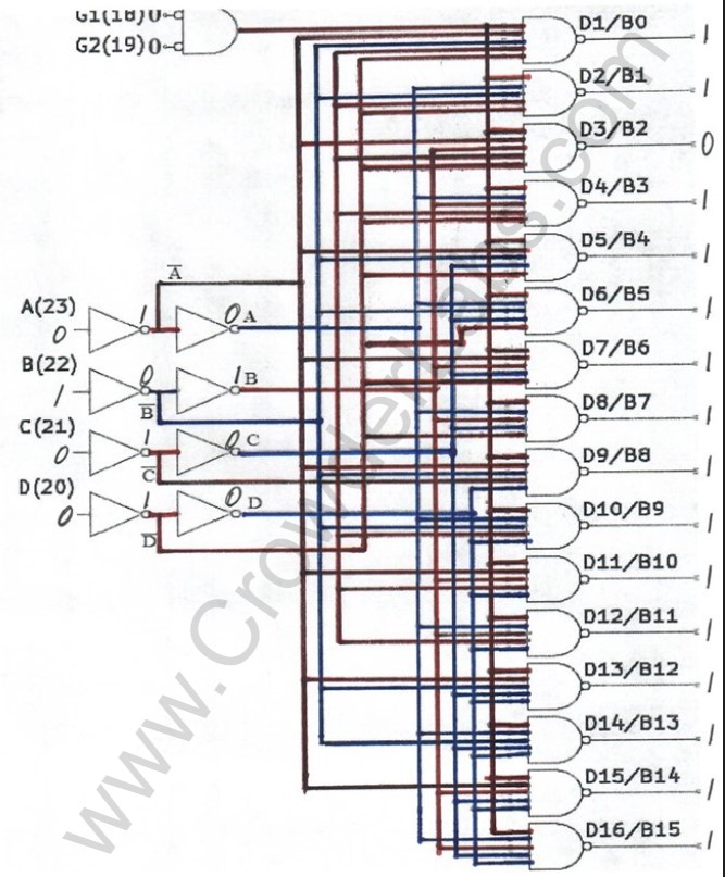
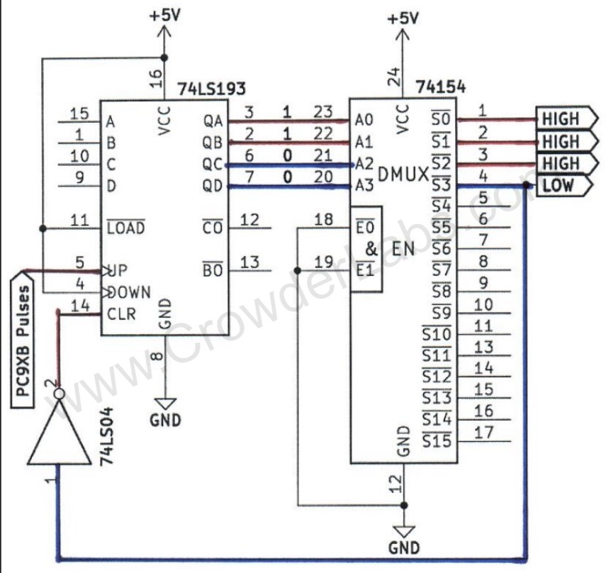
Within the next four sections, the internal operations for each channel selection are provided. The red lines are indicative of the circuits associated HIGH (1) logic states. The blue lines are indicative of the circuits associated with LOW (0) logic states.
74154 Sequence 1 - Selecting Binary Channel "0"/Decimal Channel "1":

74154 Sequence 2 - Selecting Binary Channel "1"/Decimal Channel "2":

74154 Sequence 3 - Selecting Binary Channel "2"/Decimal Channel "3":

74154 Sequence 4 - Selecting Binary Channel "3"/Decimal Channel "4":

Triple Stack Sequencing Schematic:

74193 & 74154 - Sequence 1:
As the binary counter increments, corresponding binary values are sent over the four lines as shown below. Initial state of 0000, after clear has been triggered, causing the 74154’s S0 (Channel “1”) to change from a HIGH state to LOW state as shown below.

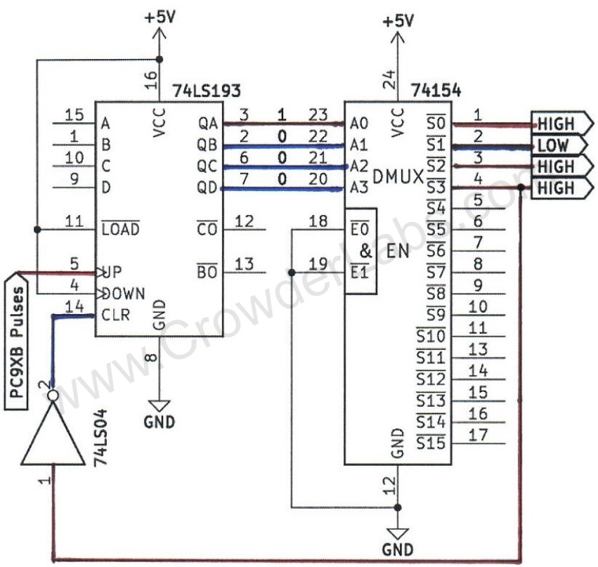
74193 & 74154 - Sequence 2:
A LOW to HIGH pulse (Pulse #1) received from the 9XB, incrementing the 74193 to a binary value of “1” (0001). This output state causes the 74154’s S1 (Channel “2”) to change from a HIGH to LOW state. Previous S0 (Channel “1”) returns back to HIGH state as shown below.

74193 & 74154 - Sequence 3:
Another LOW to HIGH pulse (Pulse #2) is received from the 9XB, incrementing the 74193 to a binary value of “2” (0010). This causes the DMUX’s output S2 (Channel “3”) to change from a resting HIGH state to LOW state. Previous S1 (Channel “2”) changes back to HIGH from triggered LOW state as shown below.

74193 & 74154 - Sequence 4:
Finally, a LOW to HIGH pulse (Pulse #3) is received from the 9XB, Incrementing the 74193 to a binary value of “3” (0011). This causes DMUX’s S3 (Channel “4”) to change from resting HIGH state to LOW state. Previous S2 (Channel “3”) returns to HIGH state from triggered LOW state as shown below.

PC9XB Pulses into hex Inverter:
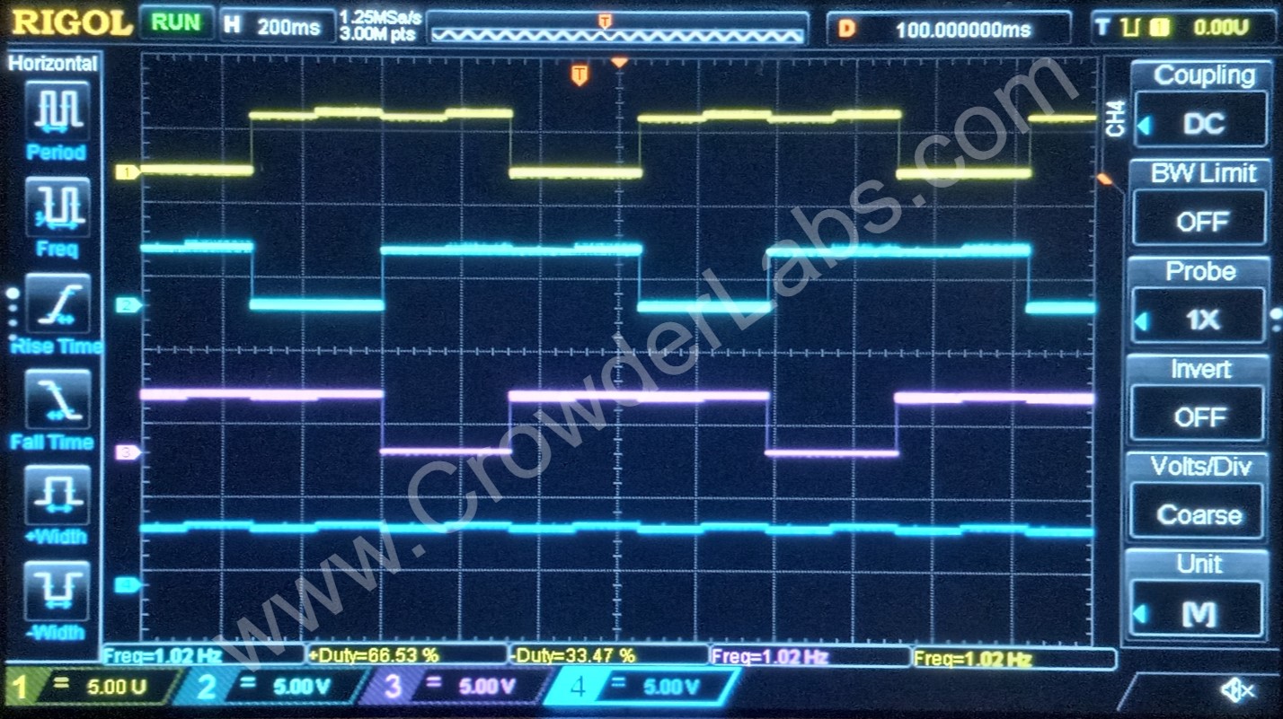
Pulse train (from PC9XB) is applied into the first hex inverter (74LS04-1) input pins #3, #5, #9, and #11. Duty cycle is a fixed at 50%. The screenshot below is provided to demonstrate the relationship between the input pulse train (Yellow), inverter input (pin #11 - Blue) and inverter output (pin #6 - Magenta).

Pulses into "COUNT UP" pin of 74193:
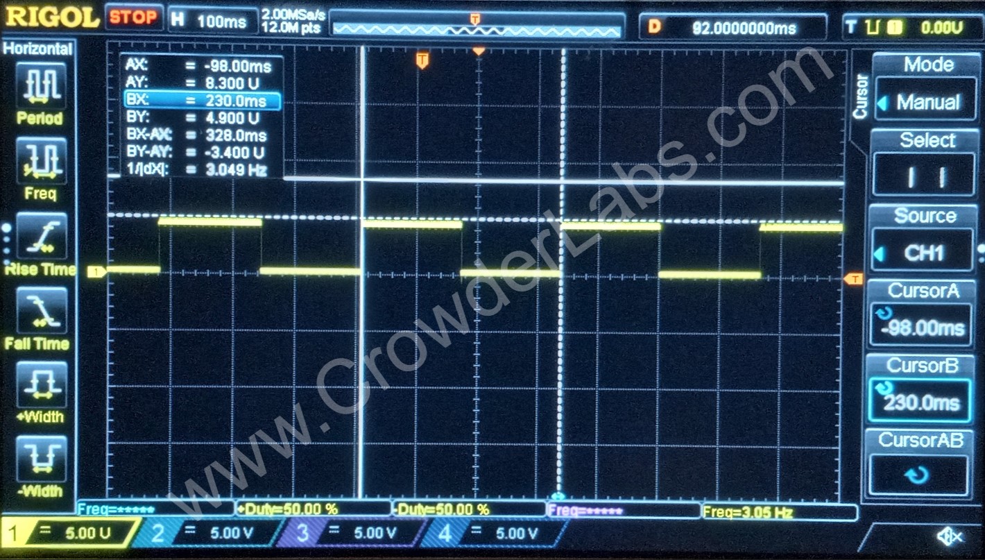
Output pin #6 increments the COUNT UP (pin #5) of binary counter (74LS193) by providing a HIGH logic state from the pulse frequency during its LOW logic state. The screenshot below shows the clock pulse applied to pin #5.

Binary bus count between 74193 & 74154:
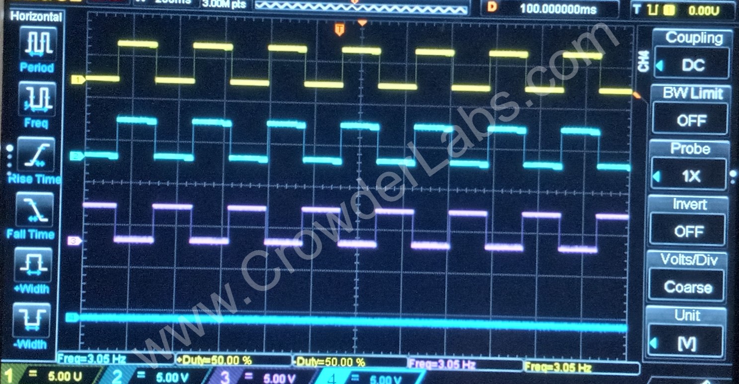
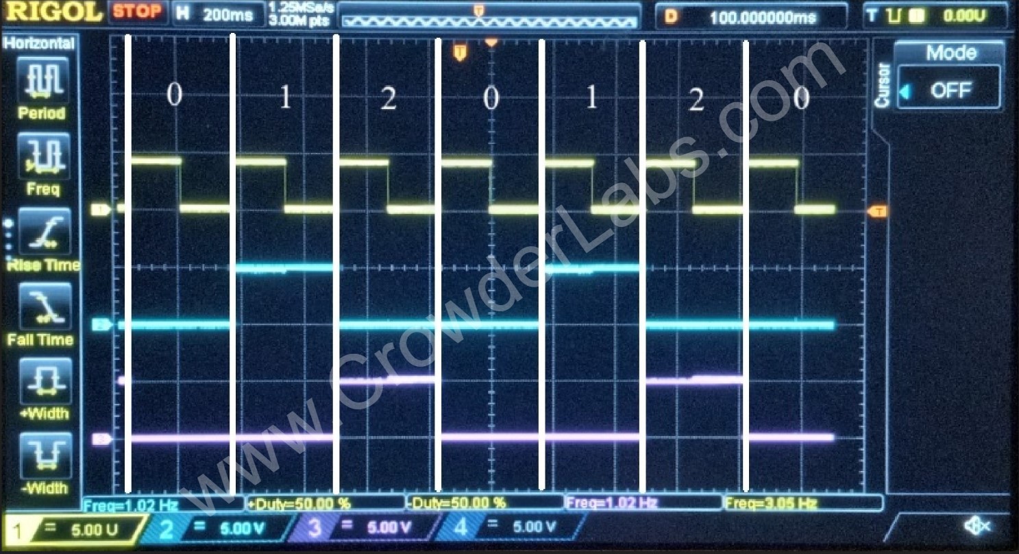
Pins #4, #11 on the 74193 are connected to (pin #16) to maintain a HIGH logic state. Due to LOAD and COUNT DOWN not being used, a HIGH logic state is maintained for operation. Binary output pins (#3[QA], #2[QB], #6[QC], and #7[QD]) count through a 4-bit binary sequence (0-3) for every low to rising edge of clock. In the screenshot below, the counting sequence is shown. Count values are divided by the white vertical lines. The counter is only counting to binary 2 (decimal “3”) with a reset on binary 3 (decimal “4”). Therefore, only two channels are utilized. Binary output [QA] is represented by the blue trace. Output [QB] is represented by the magenta trace.

Output channels of 74154:
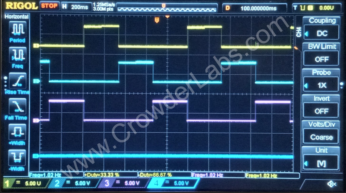
Outputs from the binary counter are communicated to the inputs of the DMUX (pin #23[A0], #22[A1], #21[A2] and #20[A3]). These cause the DMUX to select corresponding channels (pin #0[CH1], #1[CH2], and #2[CH3], #3[CH4]). When a corresponding channel is triggered, its logical state changes from a resting HIGH to LOW. Four outputs are selected in a sequential fashion. The screenshot below, illustrates the sequential manner of each channel. The first channel is represented by the yellow trace. The second channel is represented by the blue trace. The third channel is represented by the magenta trace. Finally, the fourth channel is represented by the dark blue trace, which is LOW due to being reset signal for binary counter.

74154 output channels through first hex inverter:
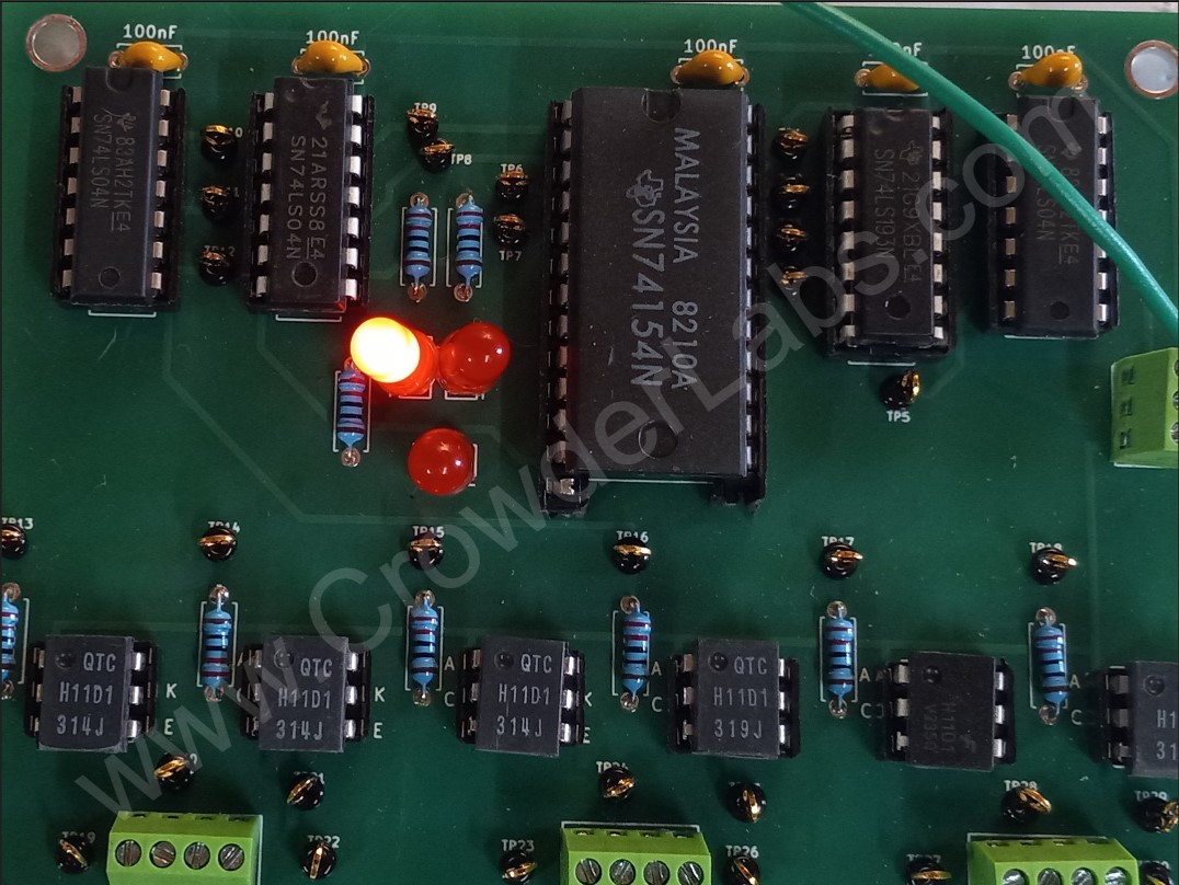
The screenshot below, shows the inversion of each 74154 channel, after passing through the second hex inverter (74LS04-2). Channel 1 is connected to input pins #1 and #13. Channel 2 is connected to input pins #3 and #11. Channel 3 is connected to input pins #5 and #9. All inputs are at a LOW logic state. Output pins #8, #10 and #12 are connected to the anode of an LED through a series resistor of 220Ω. These LEDs provide visual indication of what channel is currently on when corresponding output is in a HIGH logic state. Each LED has a 20mA current through it [5v / 220Ω = 0.020A (20mA)].

LED - Sequence 1:
Below shows the first LED illuminated, which represents output “0” (Pin #1) of the DMUX.

LED - Sequence 2:
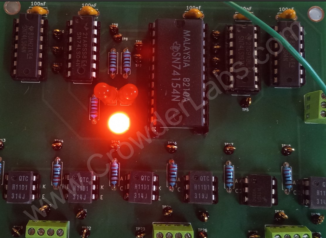
Below shows the second LED illuminated, which represents output “1” (Pin #2) of the DMUX.

LED - Sequence 3:
Below shows the third LED illuminated, which represents output “2” (Pin #3) of the DMUX.

74154 output channels through second hex inverter:
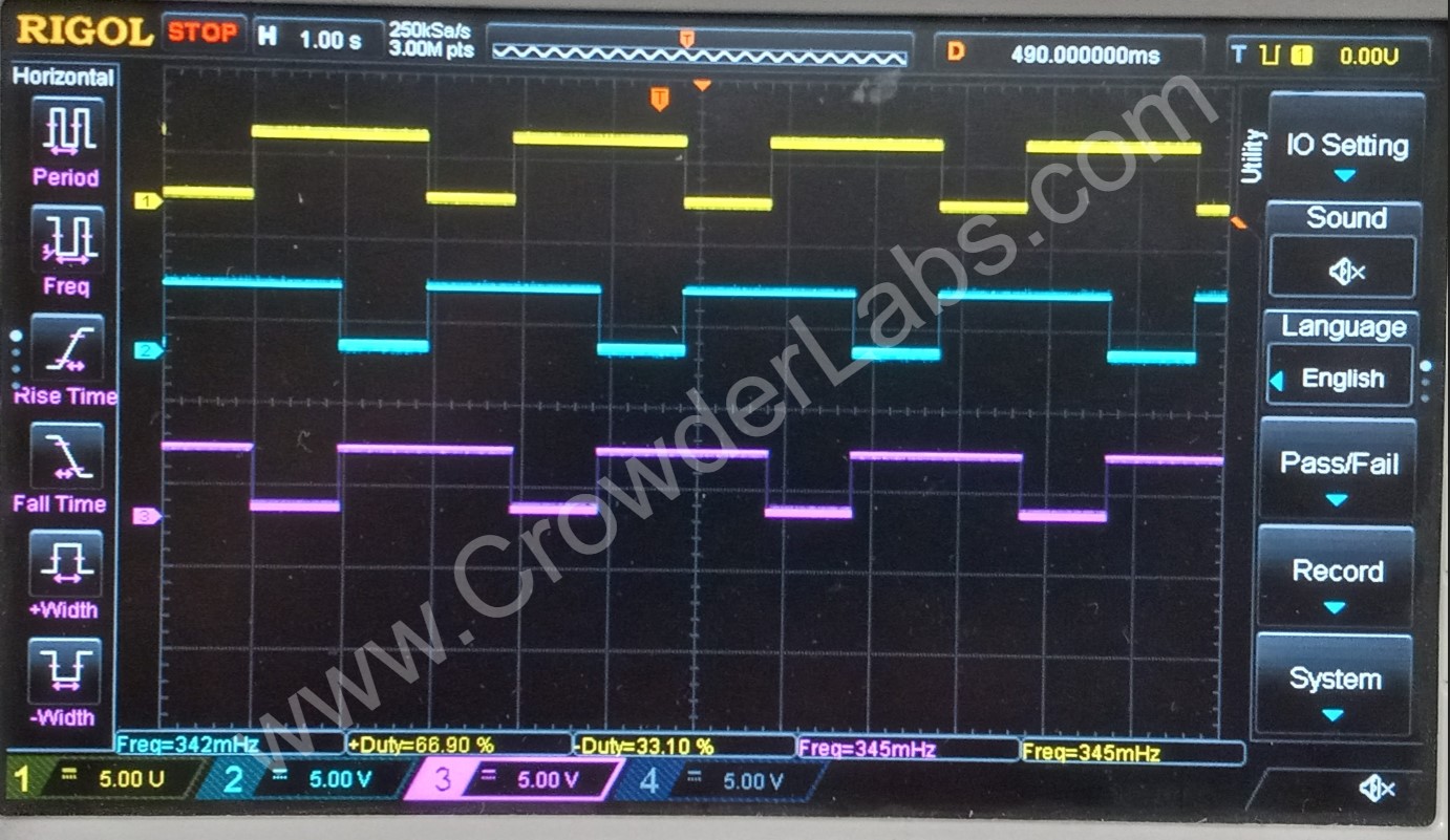
The second hex inverter, 74LS04-2, output pins: #2, #4, and #6 are connected to paired inputs on the third hex inverter 74LS04-3. The screenshot below shows the waveforms communicated to each pair of H11D1 associated with outputs from this third hex inverter. Yellow trace shows sequence 1 (binary 0) which triggers H11D1-1 and H11D1-2 via 74LS04-3 output pins #2 and #4. Teal trace shows sequence 2 (binary 1) which triggers H11D1-3 and H11D1-4 via 74LS04-3 output pins #10 and #12. Magenta trace shows sequence 3 (binary 2) which triggers H11D1-5 and H11D1-6 via 74LS04-3 pins #6 and #8. A sequential order has been maintained.

System Logic Table:
The output pins produce a LOW logic state. This LOW logic pulls down on the optocoupler cathode, turning on the internal LED. When outputs are in a HIGH logic state, the internal LED becomes reversed bias, thus keeping the LED off. The use of optocouplers provides isolation between the control circuitry and the optocoupler outputs. In simple terms, an optocoupler is a light triggered bipolar junction transistor (BJT). When the LED is turned on, the light sensitive base of the BJT causes the Collector/Emitter to come into conduction, performing the function of a switch. The amount of current conducted is related to the Current Transfer Ratio (CTR) of the optocoupler. This is similar to the gain of a regular BJT but measured as a ratio of the output current to the input current. For the H11D1, this is 20% on average. The collector and emitter of each optocoupler are connected to individual pins to allow external circuit connections. The table below details the logic continuity from the DMUX, through the hex inverters, to the optocouplers:

Logical Flow - Phase 1:

Logical Flow - Phase 2:

Logical Flow - Phase 3:

Logical Flow - Phase 4:
