Skip to main content
My Circuit Analysis
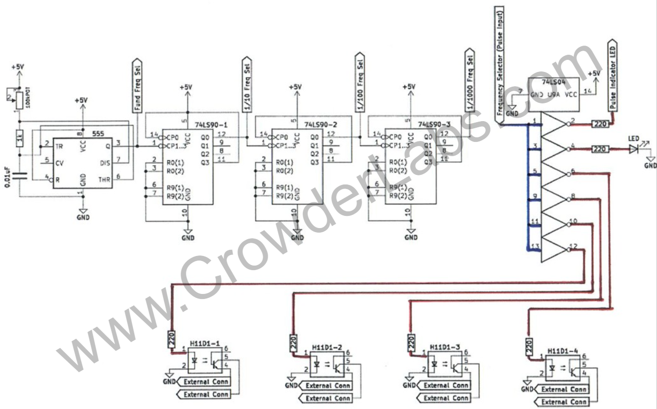
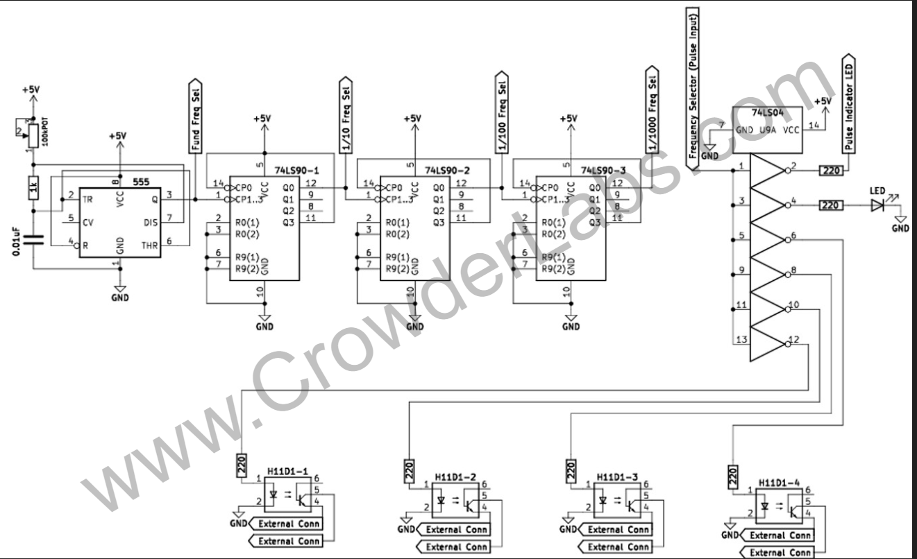
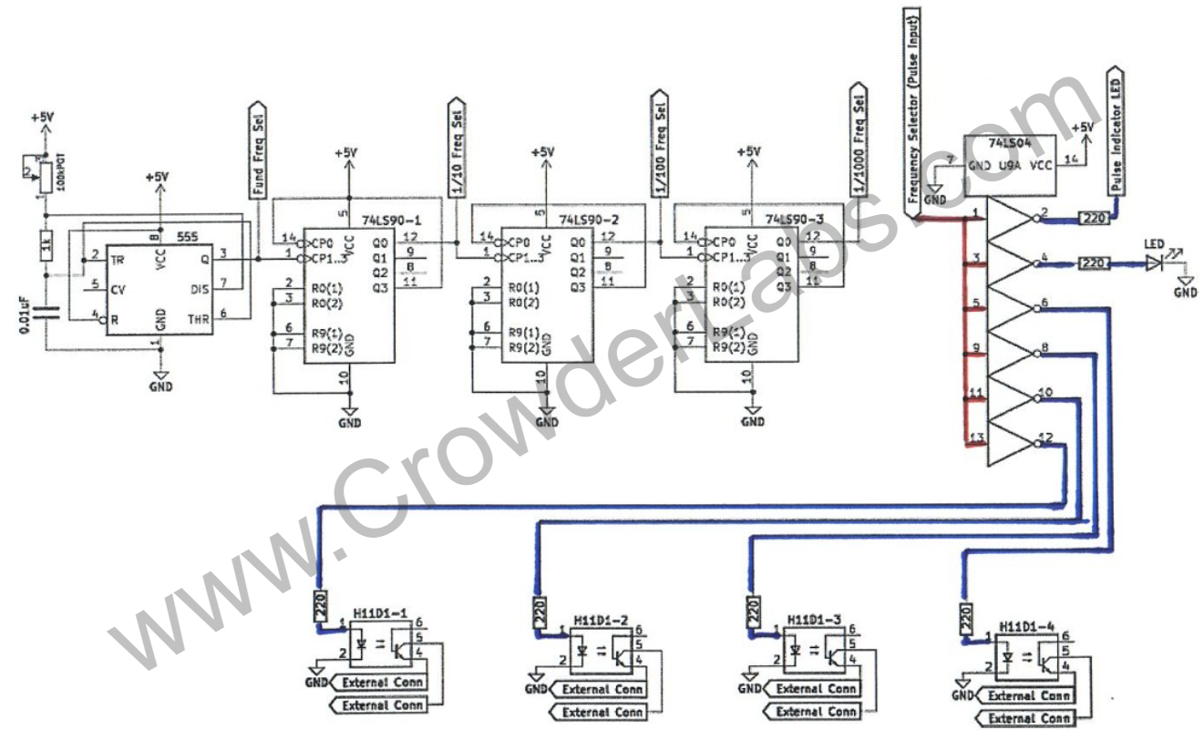
Schematic:

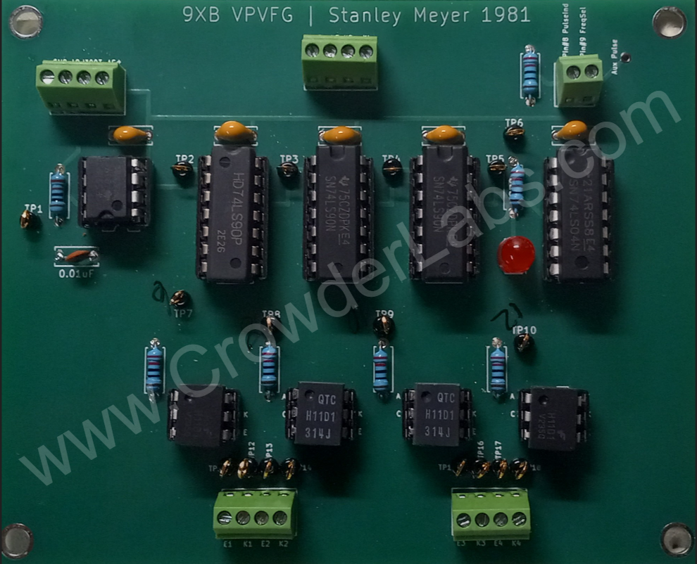
Replica PCB Top:

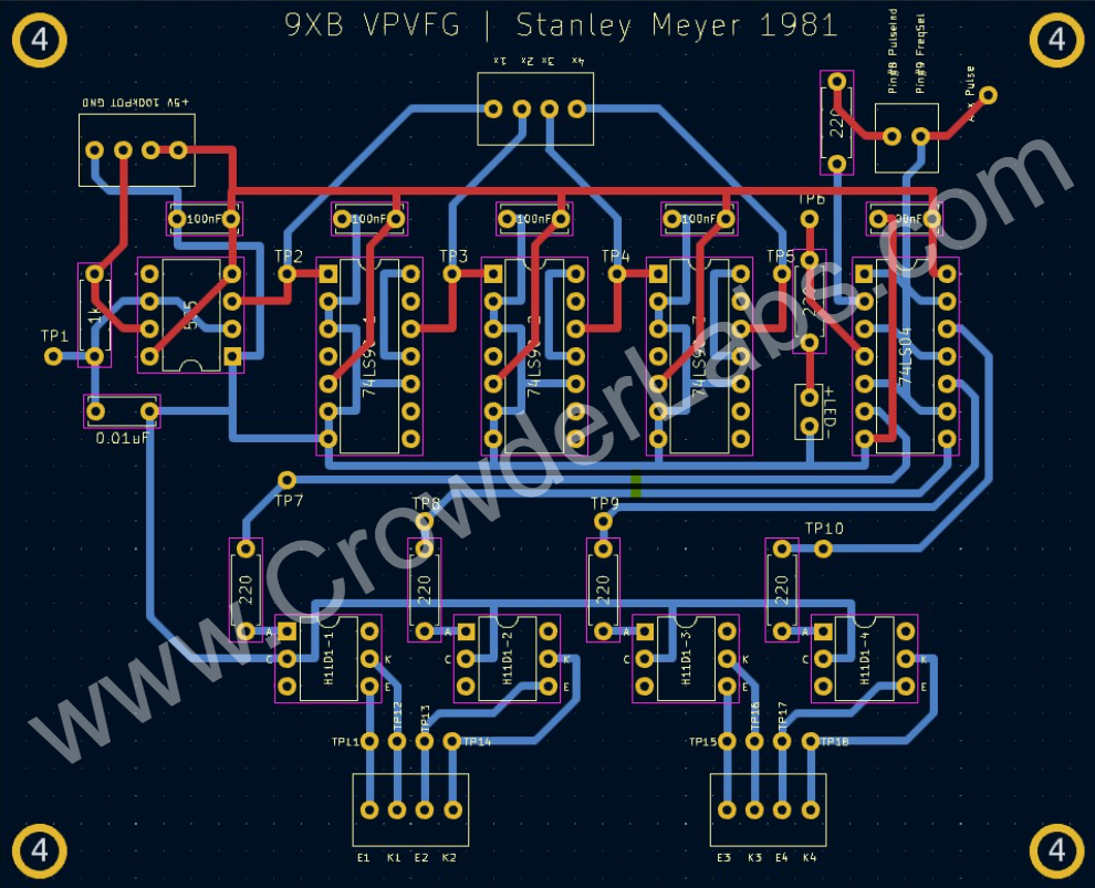
Replica PCB Traces:

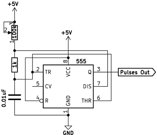
555 Operation:
The pulsing of the circuit is produced by the 555 in astable operation mode, shown in Figure 1 below. Frequency is determined by the RC time constant, produced from the values of the potentiometer (0Ω-100kΩ), R1(1kΩ) and C1(0.01uF = 10nF). As the potentiometer has its resistance varied from minimum (0Ω) to maximum (100kΩ) the time it takes to charge up C1 is varied proportionately.

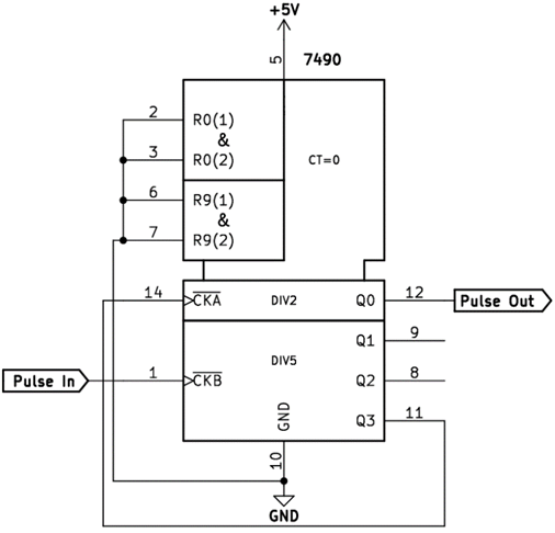
Decade Counter (7490/74LS90) Operation:
The 7490, or 74LS90 contains a divide by 2 and divide by 5 stages. These two stages are connected to form a divide by 10. Internally, networks of rising edge triggered flip flops are shifting. Figure 2 below illustrates each 7490 connections to achieve divide-by-ten operations.

Oscilloscope Waveforms:
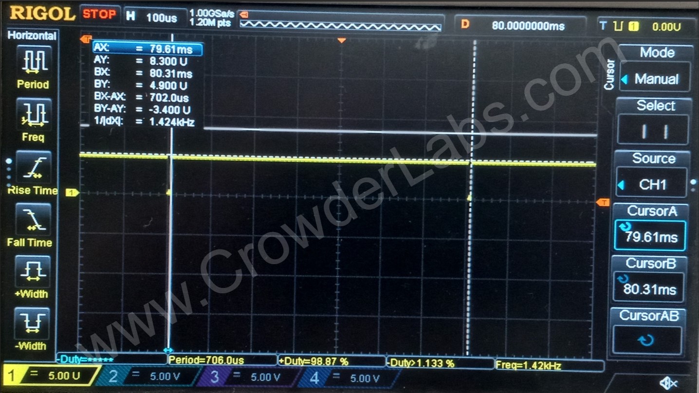
Pulse generation, supplied by the 555, produces a variable frequency output (pin #3). Given the circuit component values, varying the frequency also leads to a variance in duty cycle. Figure 3 below shows the measured duty cycle of ~1kHz. Scope measures 98.87% HIGH and 1.13% LOW.

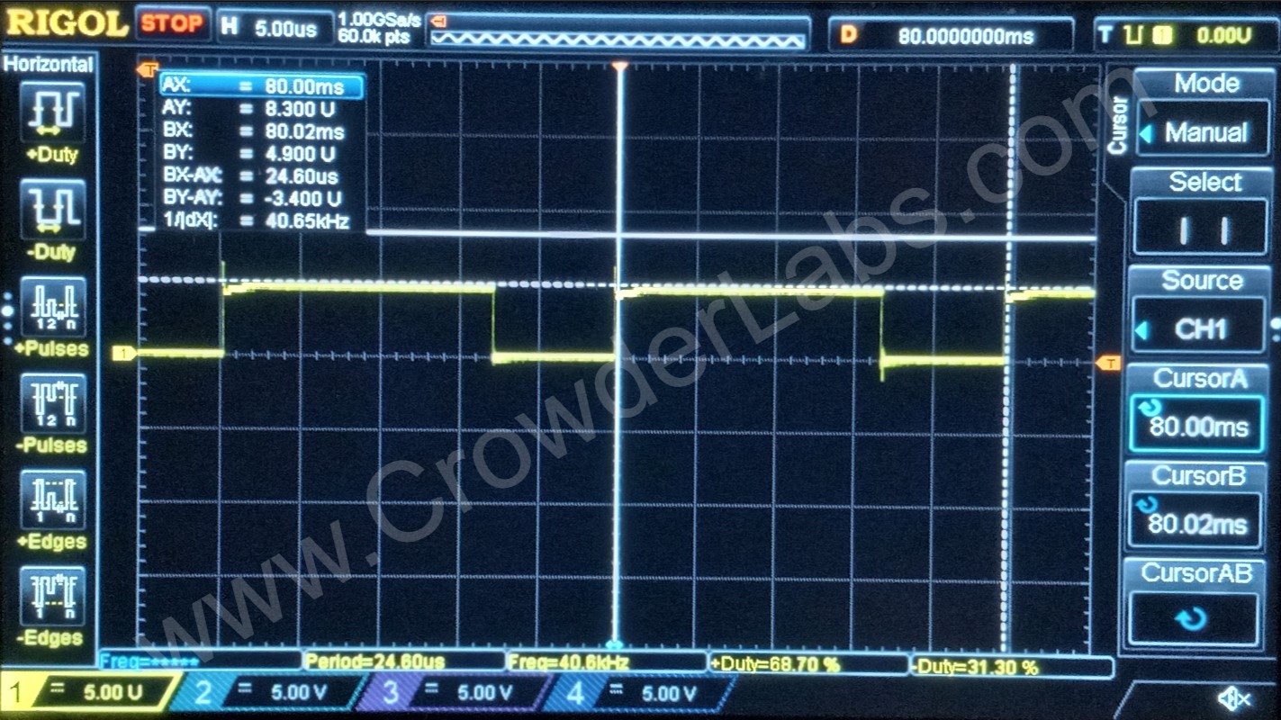
Below shows the duty cycle measurement of the fundamental frequency adjusted to ~40kHz. Scope measures 68.70% HIGH and 31.30% LOW.

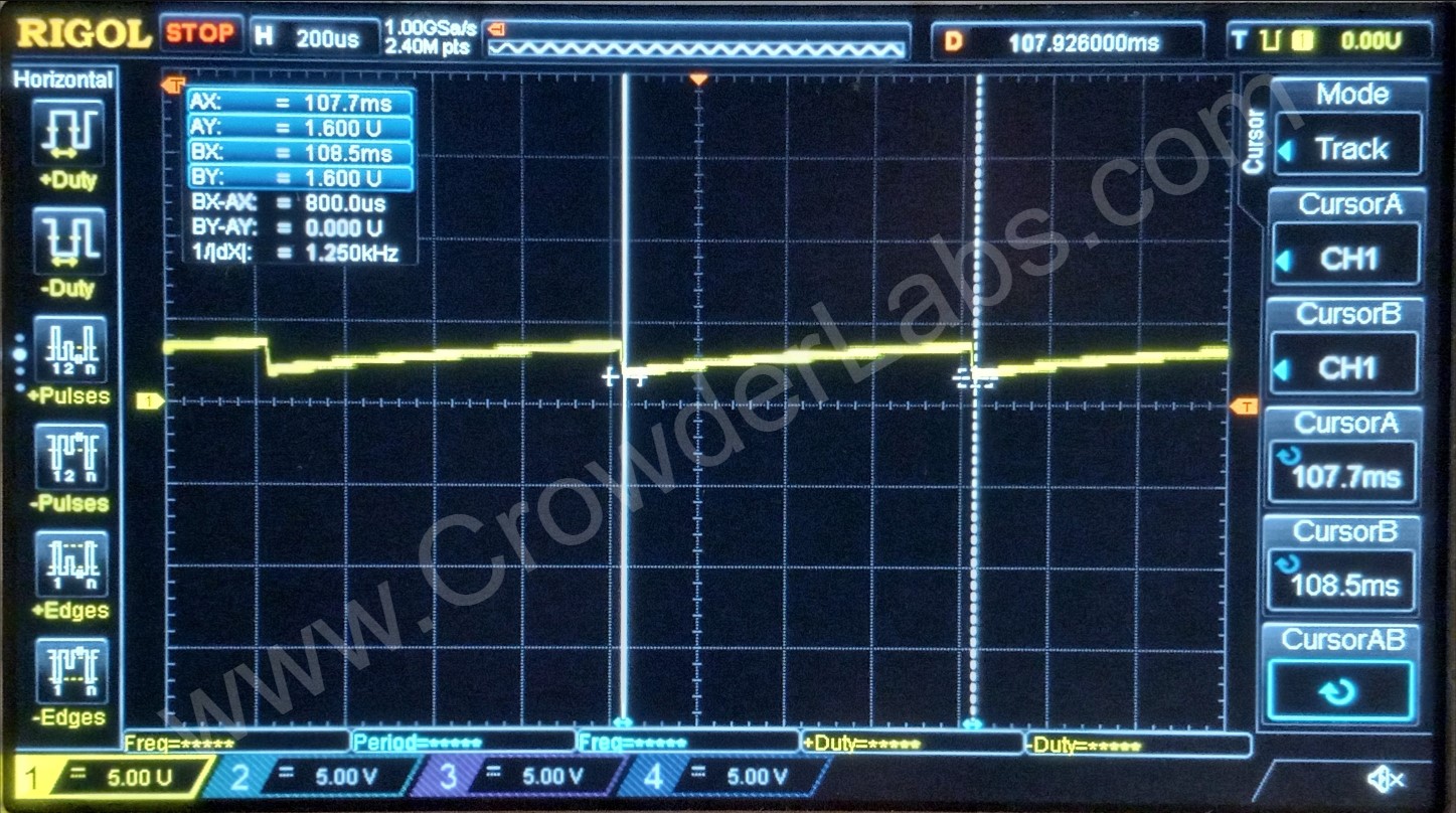
Frequency of the pulse is related to the period of the RC curve. Components of the RC curve (potentiometer and capacitor (0.01uF) determine this period. Figure 5 below demonstrates the longer period (800uS) for a lower frequency. In this capture, the frequency is 1.25kHz. To derive frequency from the period, the formula F = 1/T is utilized. Where ‘T’ is representative of the period time value. Therefore: F = 1 / 0.000800S, F = 1,250Hz.

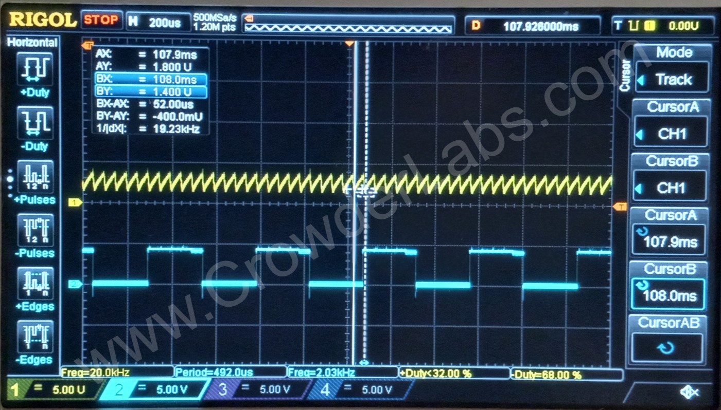
The picture below demonstrates the RC curve for a higher frequency. In this capture, the frequency is ~20kHz. Higher frequencies have lower period time values. Notice that both scope shots are on the same time base, 200uS per division. This was intentionally done to show how the RC curve is occurring much faster compared to the 1.25kHz scope shot above. Comparing the two further demonstrates the linear relationship between RC charging time and frequency.

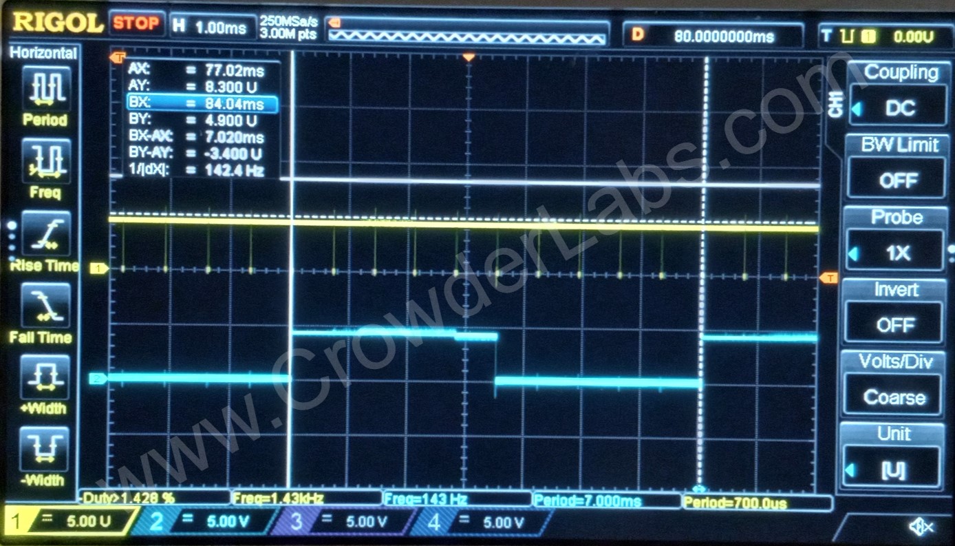
The 555 output (pin #3) frequency enters into the input (pin #1) of the first binary counter (74LS90-1), which is in a divide-by-ten arrangement. The counter begins the process of dividing the fundamental frequency by ten and conditioning the duty cycle to a fixed 50%. The output (pin #12), provides a frequency that is ten times less (1/10) that of the fundamental, and an external tap for selection of this frequency. The picture below captures this first division. Channel one (yellow trace) shows the fundamental frequency as discussed earlier. Channel two (blue trace) shows the divided-by-ten frequency. Channel one has a measured frequency of 1.43kHz and a period of 700uS. Channel two has a measured frequency of 143Hz and period of 7mS. Finding the quotient between these two, the measurements are ten divisions between one another: 1,430Hz / 143Hz = 10; 7mS / 700uS = 10. This frequency output (143Hz) is connected with the input (pin #1) of the second divide-by-ten counter (74LS90-2).

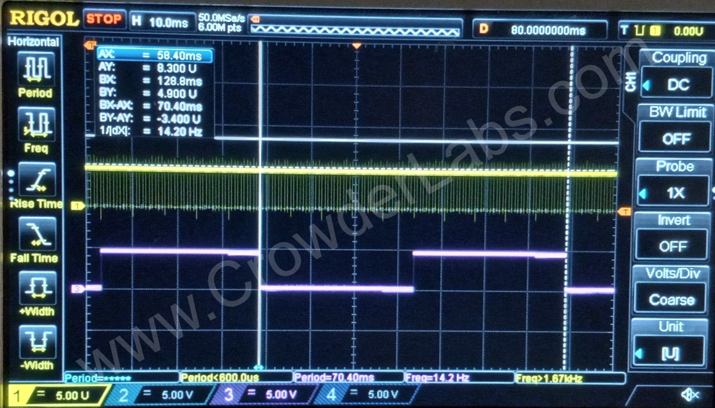
This second counter begins the process of dividing the fundamental frequency by one hundred. The output pin (#12), provides a frequency that is one hundred times (1/100) less than that of the fundamental. Another external tap is provided for selection of this frequency. As shown in Figure 8 below, channel one (yellow) represents the fundamental. Channel three (magenta) represents the division of one-one hundredth. The fundamental frequency is measured at 1.42kHz. The one-one hundredth division is measured at 14.20Hz.

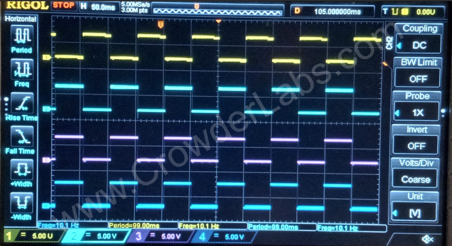
Below is a scope shot showing a comparison between all four channels.

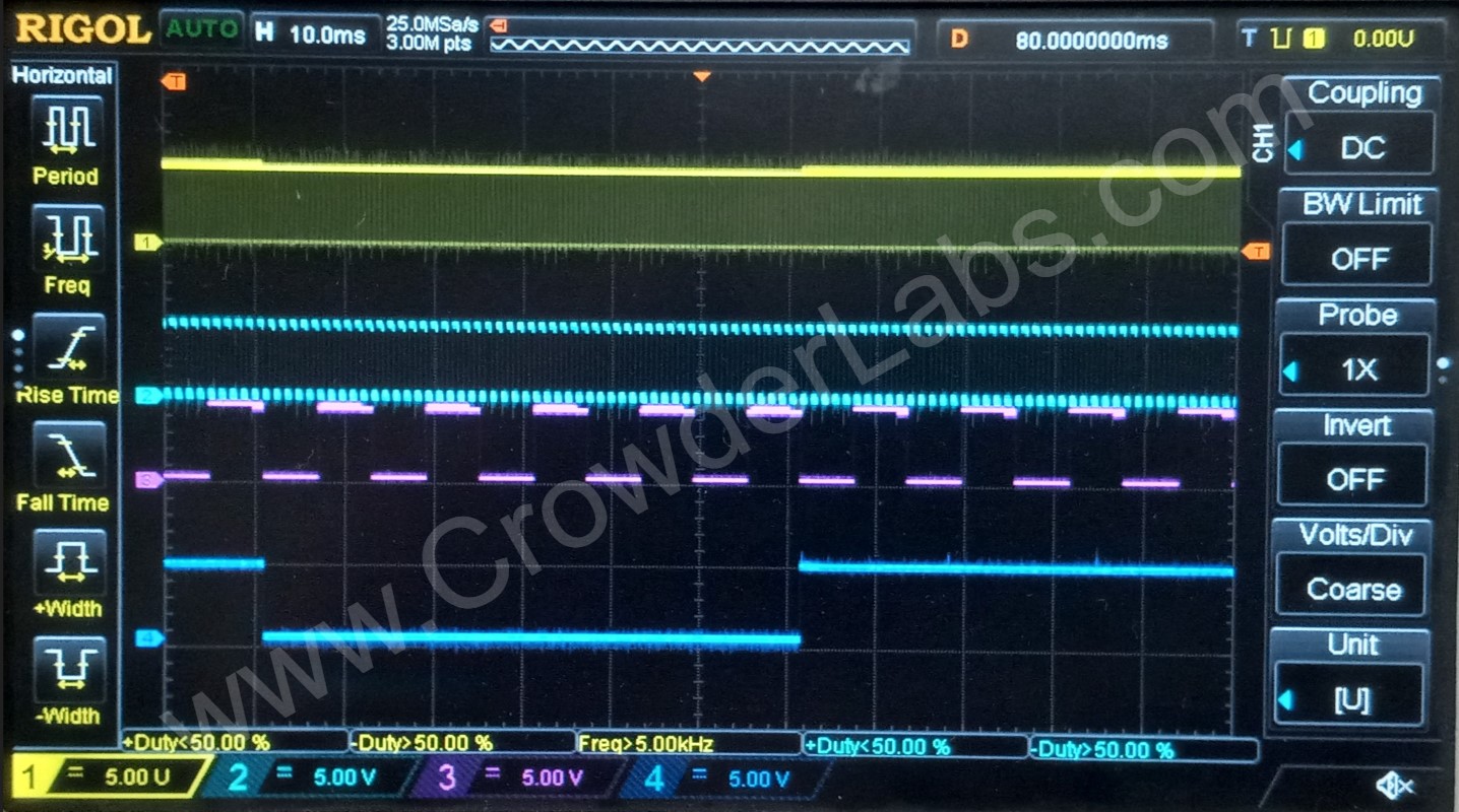
A rotary switch provides the input, of whichever frequency is desired, into the inputs (pins #1, #3, #5, #9, #11, #13) of the hex inverter (74LS04). All of the inputs are connected together to synchronize the associated outputs. These outputs are logically inverted from the input pulse polarity as shown below. The input channel is represented by yellow trace. Other traces represent outputs to three of the four optocouplers.

First output (pin #2) is connected to a series 200Ω, ¼ watt resistor which provides current limiting (20mA) to the cathode of an externally mounted LED. This external LED provides visual indication of the frequency received by the optocouplers. Second output (pin #4) is connected to a series 200Ω, ¼ watt resistor which provides current limiting (20mA) to the cathode of the PCB mounted LED. This LED provides visual indication of the frequency received by the optocouplers. Four other outputs (pins #6, #8, #10, #12) are connected to a series 200Ω, ¼ watt resistor which provides current limiting (20mA) to the anode of their respective optocouplers (H11D1-1, H11D1-2, H11D1-3, H11D1-4).
When the 74LS04 output logical states are HIGH (1), the associated optocoupler’s internal LED turns on, which influences the base of the transistor, producing conduction on the output side. Conversely, when the 74LS04 output logical state are LOW (0), the associated optocoupler internal LED turns off, having been reversed biased. The optocouplers perform electrical isolation between the pulsing circuitry and their respective output terminals. The four optocouplers are used to provide pulsing for other circuitry that will be expanded upon in other sections. The schematic details which pin number is associated with the collector and emitter of the associated optocoupler.
Logical Flow - Phase 1:

Logical Flow - Phase 2:
